| Aug 27, 2022 |
Weaving atomically thin seams of light with in-plane heterostructures
(Nanowerk News) Researchers from Tokyo Metropolitan University have developed a way to produce high quality monolayers of a selection of different transition metal dichalcogenides which meet over an atomically thin seam.
|
|
By coating this layer with an ion gel, a mixture of an ionic liquid and a polymer, they could excite light emission along the seam. The light was also found to be naturally circularly polarized, a product of the customizable strain across the boundary.
|
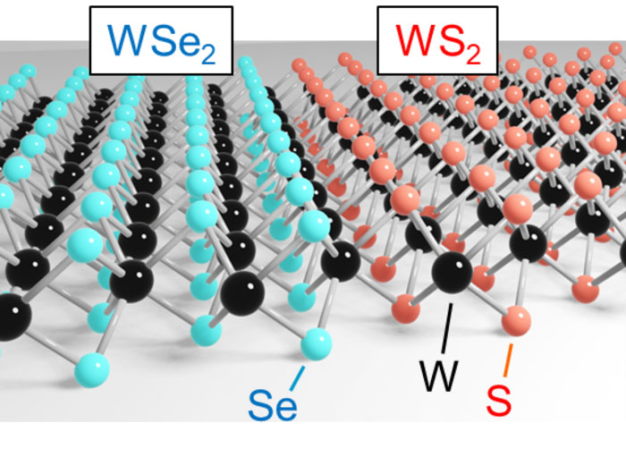 |
| Tungsten diselenide and tungsten disulfide monolayers combine over an atomically thin seam in an in-plane heterostructure. (Image: Tokyo Metropolitan University)
|
|
The team reported thir findings in Advanced Functional Materials ("Efficient and Chiral Electroluminescence from In-Plane Heterostructure of Transition Metal Dichalcogenide Monolayers").
|
|
Light-emitting diodes (LEDs) have become ubiquitous through their revolutionary impact on nearly all forms of lighting. But as our needs diversify and performance demands grow, there is still a clear need for even more power efficient solutions.
|
|
One such option involves the application of in-plane heterostructures, where ultra-thin layers of different materials are patterned onto surfaces to produce boundaries.
|
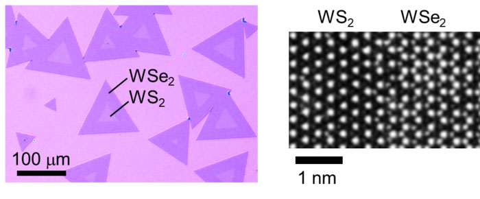 |
| (left) Tungsten disulfide and tungsten diselenide regions observed using optical microscopy. (right) Scanning transmission electron microscopy (STEM) image of the boundary between the two different TMDCs. (Image: Tokyo Metropolitan University)
|
|
In the case of LEDs, this is where electrons and “holes” (mobile voids in semiconducting materials) recombine to produce light. The efficiency, functionality, and scope of applications for such structures are determined not only by the materials used but by the dimensions and nature of the boundaries, which has led to a great deal of research into controlling their structure at the nanoscale.
|
|
A team of researchers led by Associate Professor Yasumitsu Miyata of Tokyo Metropolitan University, Assistant Professor Jiang Pu and Professor Taishi Takenobu of Nagoya University have been investigating the use of a class of materials known as transition metal dichalcogenides (TMDCs), a family of substances containing a group 16 element from the periodic table and a transition metal.
|
|
They have been using a technique known as chemical vapor deposition to controllably deposit elements onto surfaces to create atomically thin monolayers; much of their work has been to do with how such monolayers can be varied to create patterns with different regions made of different TMDCs.
|
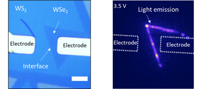 |
| (left) Optical microscope image of an in-plane heterostructure with two electrodes attached. (right) Once a voltage is applied, light is seen to be emitted from the interface between the two different TMDCs. (Image: Tokyo Metropolitan University)
|
|
Now, the same team have succeeded in significantly refining this technology. They redesigned their growth chamber so that different materials could be moved closer to the substrate in a set sequence; they also introduced additives to change the vaporization temperature of each component, allowing for optimized conditions for the growth of high-quality crystalline layers.
|
|
As a result, they succeeded in using four different TMDCs to create six different types of sharp, atomically thin “seams.” Furthermore, by adding an ion gel, a mixture of an ionic liquid (a fluid of positive and negative ions at room temperature) and a polymer, a voltage could be applied across the seams to produce electroluminescence, the same basic phenomenon underlying LEDs.
|
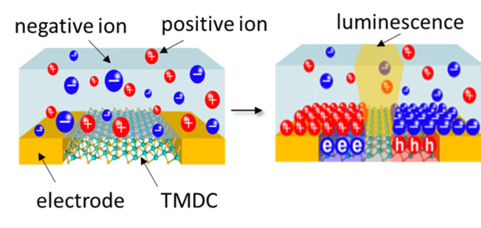 |
| Positive and negative ions in the ionic liquid are mobile even while the polymer network keeps the gel rigid. When a voltage is applied, ions migrate and induce the transport of electrons and holes, which in turn recombine at the interface to create light. (Image: Tokyo Metropolitan University)
|
|
The customizability of their setup and the high quality of their interfaces makes it possible to explore a wide range of permutations, including different degrees of “misfit” or strain between different TMDCs.
|
|
Interestingly, the team discovered that the boundary between a monolayer of tungsten diselenide and tungsten disulfide produced a “handed” form of light known as circularly polarized light, a direct product of the strain at the seam. This new degree of control at the nanoscale opens up a world of possibilities for how their new structures may be applied to real devices, particularly in the field of quantum optoelectronics.
|

