| Oct 20, 2022 |
Confining classical and quantum waves with crystals
(Nanowerk News) Manipulating elusive waves like light, sound or electrons, in periodic structures or crystals, has something mysterious. We already know that confining waves is possible by deliberately introducing tailored deviations from perfect periodicity into the crystal. But how exactly are the waves locked up? Are they confined in all dimensions simultaneously, or do they retain the freedom to move along a line or in a plane?
|
|
Remarkably, the key step from having the crystal’s structure to predicting the confinement of waves had not been taken until now. A team of researchers from the University of Twente now describe how any kind of wave, whether quantum or classical, is confined in any kind of crystal. The results will notably boost efficient new integrated circuits that steer information encoded in tiny light pulses through smart cities.
|
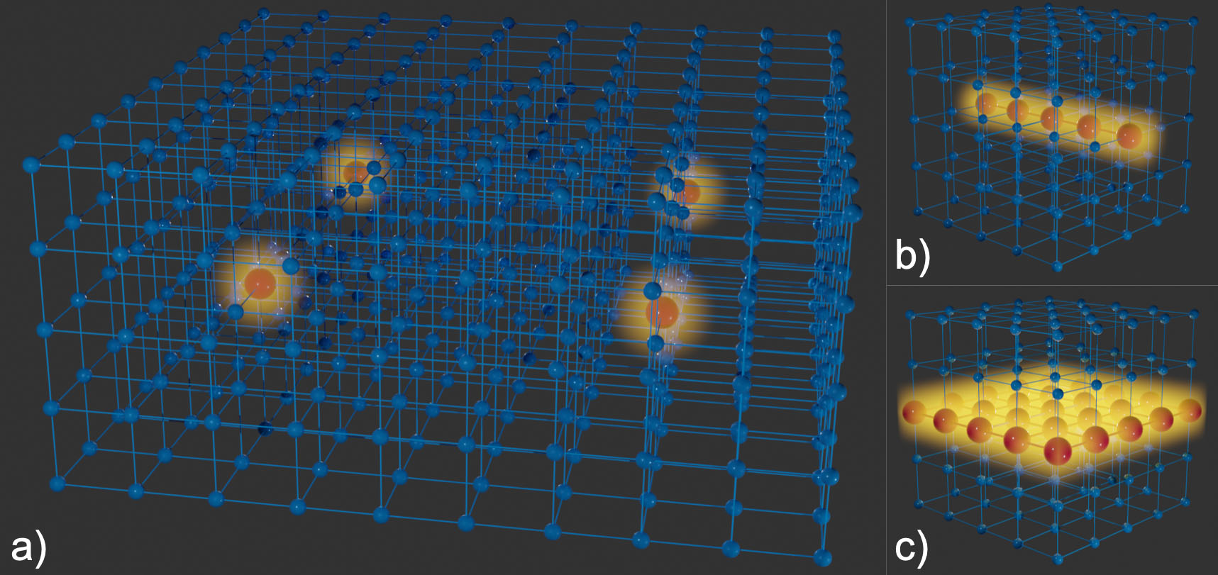 |
| Figure 1: Illustration of a 3-dimensional crystal with various types of confining centers. Blue spheres represent unmodified unit cells, and red spheres are confining centers. (a) Crystal with four confining centers, each trapping waves (yellow) in all three dimensions (c=3) simultaneously. (b) Crystal with a linear confining center where waves can propagate in 1 dimension, analogous to an optical fiber (c=2). (c) Crystal with a planar confining center where waves can propagate in 2 dimensions, analogous to a 2D electron gas (c=1). (Image courtesy of the researchers)
|
|
Waves represent an inseparable part of our everyday life, whether we listen to music, observe our reflection in a mirror, use our mobile phone, or experience the ocean rocking a sailing ship. A central challenge in manipulating waves for applications requires the ability to confine the waves in small regions in space. Such a confinement can be achieved with the help of crystals.
|
|
Many people are familiar with crystals formed by minerals in nature. Such crystals can be used to confine quantum-mechanical electronic waves. Man-made crystals of silicon have led in 1947 to the discovery of electronic transistors, the basis for the ongoing digital revolution. We now know that there are other types of crystals, that are able to confine and manipulate different type of waves like light, sound, and potentially even earthquakes.
|
|
Having a crystal at hand is, however, not enough to achieve wave confinement. The internal structure of the crystal must specifically suit the desired application. To make matters more complicated, there are infinite possibilities for this structure, considering all conceivable building blocks and their arrangements in the crystal. Until now, scientists and engineers trying to confine waves had to rely on their intuition, guesswork, and costly trial-and-error experiments to design sufficiently good crystals for each desired application.
|
Generic approach
|
|
In their Physical Review Letters paper ("Scaling theory of wave confinement in classical and quantum periodic systems"), the Twente researchers present a robust analysis tool that predicts how waves are confined within a crystal, using only the crystal’s structure as input.
|
|
First author and PhD student Kozon explains: “A central parameter in our analysis is a ‘confinement dimensionality’ that we have newly invented. It describes the confinement for each possible wave.”
|
|
COPS group leaders Vos and Lagendijk add enthusiastically: “We got excited when we realized from discussions with Marek that our method pertains to not only to classical waves such as sound and light, but also to quantum waves such as electrons in tiny nanostructures.”
|
|
Based on the new know-how, the designers of crystals can now benefit from new ‘rules of thumb’ for specific applications, resulting in highly simplified and thus efficient design processes.
|
|
MACS group leaders Schlottbom and van der Vegt add: “Our results are relevant for efficient information processing in new photonic and electronic chips that will populate future smart cities.”
|
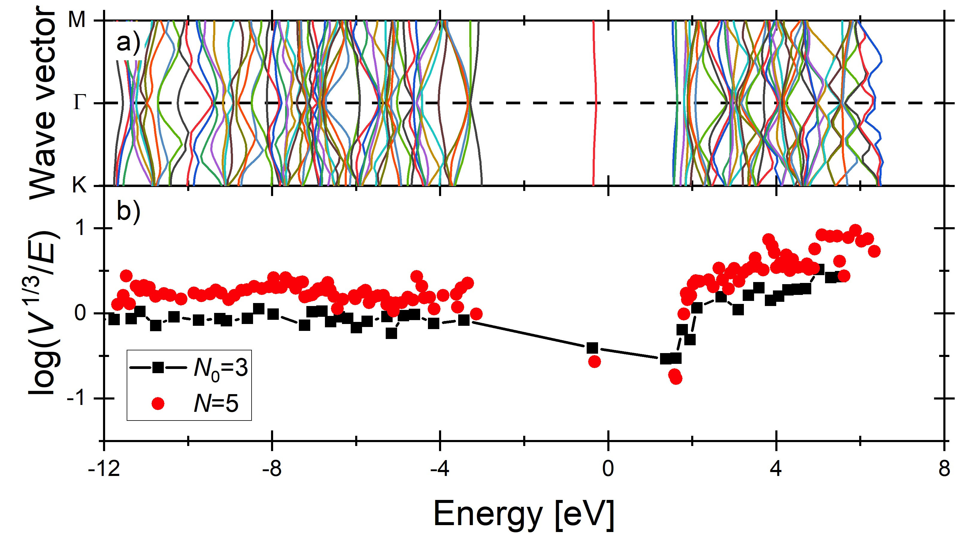 |
| Figure 2: Confinement analysis of a 2-dimensional quantum crystal for electrons in the semiconductor hexagonal boron-nitride with a nitrogen vacancy. (a) Dispersion relations of the crystal. (b) Ratio of the confinement volume to confinement energy computed for each propagating band of waves. Red points correspond to bands in the crystal with size N = 5, and black points represent the smaller reference N0 = 3 crystal. With the increased size, bands with c=2 confinement move down and bands with c=0 move up in the graph and are thus clearly distinguished. Due to the wave confinement geometry, it turns out there are no c=1 bands. (Image courtesy of the researchers)
|
|
This research was done in the groups Complex Photonic Systems (COPS) and Mathematics of Computational Science (MACS), both part of UT’s MESA+ Institute for Nanotechnology. COPS is pleased to announce that the data used for the publication is available in the public Zenodo database.
|

