| Jul 24, 2023 |
Spin defects in hexagonal boron nitride created by helium ion bombardment(Nanowerk News) National University of Singapore (NUS) physicists have developed a method using a focused beam of helium ions to create arrays of defects in hexagonal boron nitride (hBN) that can potentially be used for magnetic sensing applications. |
| Hexagonal boron nitride (hBN) is a two-dimensional (2D) material comprising of boron and nitrogen atoms arranged in a hexagonal lattice structure. It exhibits unique properties for applications in quantum sensing. Many types of defects have been discovered in hBN and one of them, the negatively charged boron vacancy (VB–), is of particular interest as it possesses spin properties that make it valuable for quantum sensing applications. |
| In this study, a beam of high energy helium ions produced at the accelerator facility at the Centre for Ion Beam Applications (CIBA) in the Department of Physics, NUS was used to irradiate flakes of hBN to generate VB– optical centres (schematically shown in Figure 1a). The ability to focus the ion beam to nano-sized spots and to spatially scan the beam allows for patterned arrays of optical emitters to be fabricated with high precision. Figure 1b shows a photoluminescence map of an irradiated region in the hBN flake. |
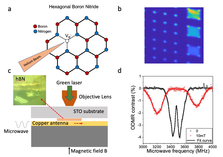 |
| Figure 1: (a) Schematic of the negatively charged boron vacancy (VB–) optical defect centre in hexagonal boron nitride (hBN), (b) Photoluminescence map of an array of VB– optical defects produced on a hBN flake. (c) Experimental setup for performing Optically Detected Magnetic Resonance (ODMR) measurements. (d) ODMR spectrum from the VB– defects showing the resonant dips measured with zero and 10 mT magnetic fields applied. (Image: Nsational University of Singapore) |
| The work is the result of a collaboration between a research team led by Associate Professor Andrew BETTIOL and the team led by Associate Professor Goki EDA#, both from the Department of Physics, NUS. The VB– optical defect centre which, was produced through the experiments run by the research team, shows some interesting properties when it is exposed to microwave energy. |
| This study was published in the journal Advanced Optical Materials ("High Sensitivity Spin Defects in hBN Created by High-Energy He Beam Irradiation"). |
| A spectroscopic technique known as Optically Detected Magnetic Resonance (ODMR) was used to sense tiny magnetic fields in the experiments. This technique combines the principles of magnetic resonance and optical spectroscopy to study the properties of paramagnetic materials and their interaction with electromagnetic radiation. A schematic of the experimental step used is shown in Figure 1c. First, a green laser is used to excite the VB– defect centre so that it emits light at a wavelength of around 810 nm, which is in the near infra-red part of the electromagnetic spectrum. A copper antenna is then used to generate a specific microwave frequency near the hBN sample. This microwave energy initializes the defect into a spin state that results in the reduction in the light intensity emitted by the defect. The microwave frequency is tuned until a drop in light intensity is detected. This happened at approximately 3.48 GHz, where a double dip in the photoluminescence intensity was observed (shown in Figure 1d). Once the microwave resonance frequency is found, the sensor is ready for use to detect magnetic fields. |
| Prof Bettiol said, “By using this unique property exhibited by hBN, a tiny magnetic field that sometimes occurs in biological systems or in magnetic materials will shift the resonant frequency and this will cause the light emission from the sensor to be restored. The light emission from the VB– optical defect centre provides a means of optically detecting the local magnetic field.” |
| Prof Eda added, “hBN is a versatile material that can be readily integrated into on-chip devices. Our demonstration to create spin defects in hBN with high precision is an important step towards realizing on-chip magnetic sensors.” |
| Source: National University of Singapore (Note: Content may be edited for style and length) |

