| Nov 10, 2023 |
Probing the intricate structures of 2D materials at the nanoscale
(Nanowerk News) Two-dimensional (2D) materials, composed of a single or a few layers of atoms, are at the forefront of material science, promising revolutionary advancements in technology. These ultra-thin materials exhibit unique and exotic properties, particularly when their layers are stacked and twisted in specific ways.
|
|
This manipulation of layers can significantly alter their electronic characteristics, presenting exciting opportunities for the development of next-generation technologies such as more efficient computers and reliable electricity storage systems.
|
|
Understanding the intricate relationship between the atomic structure and electronic properties of these materials, however, poses a significant challenge. Traditional microscopy techniques struggle to capture the complete 3D atomic structure of these layered materials, especially when the layers are oriented differently or composed of light elements.
|
|
This is where the novel operating mode of interferometric four-dimensional scanning transmission electron microscopy (4D-STEM) comes into play.
|
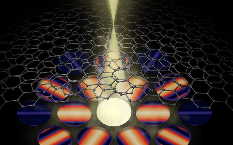 |
| A convergent electron beam in a scanning transmission electron microscope interacts with a twisted bilayer of graphene (carbon), generating intricate disk-shaped intensity patterns that encode the precise local atomic arrangement. (Image: Oak Ridge National Laboratory)
|
|
Developed by researchers at Oak Ridge National Laboratory, this advanced microscopy technique allows for an unprecedented examination of layered 2D materials. It enables scientists to measure atomic-scale structural distortions, twist angles, and interlayer spacings, which are crucial for understanding and harnessing the unique electronic properties of these materials.
|
|
Unlike conventional methods, interferometric 4D-STEM utilizes a defocused electron probe based on Bragg interferometry, providing detailed insights into the relative positions of atoms within separate layers.
|
|
This technique has already demonstrated its capabilities in studies with bilayer and trilayer graphene, showcasing how it can illuminate the intricate interplay between structural arrangements and electronic properties in few-layered 2D materials.
|
|
By offering a window into the local structural deformations within layers, the direction and magnitude of twists between layers, and the distances between them, interferometric 4D-STEM opens new avenues for the design and development of materials with bespoke properties.
|
|
This breakthrough in microscopy is not just a leap forward in understanding layered 2D materials, but also a critical step towards realizing their full potential in advancing modern technology.
|
|
The research has been published in Small ("Interferometric 4D-STEM for Lattice Distortion and Interlayer Spacing Measurements of Bilayer and Trilayer 2D Materials").
|

