| Feb 07, 2024 |
Advanced measurements unravel nanoscale phenomena(Nanowerk News) Semiconductor 2D materials are a few atoms thick, and some of them exhibit localised emission, where light is emitted from such a small part of the layer that only one photon at a time is produced. This localised emission has unique properties and is vital to new quantum technologies especially in optoelectronic and quantum device applications. |
| Research has shown that stretching a 2D material called tungsten diselenide can result in localised emission, many efforts have sought to create nanostructures with the maximum strain in the layer. However, advanced measurements at NPL indicate that bending the material can have a similar effect. |
| In recently published work (Science and Technology of Advanced Materials, "Curvature-enhanced localised emission from dark states in wrinkled monolayer WSe2 at room temperature"), scientists at NPL propose that curvature of 2D material resulting from wrinkles in the 2D layer is a better way to engineer the properties. |
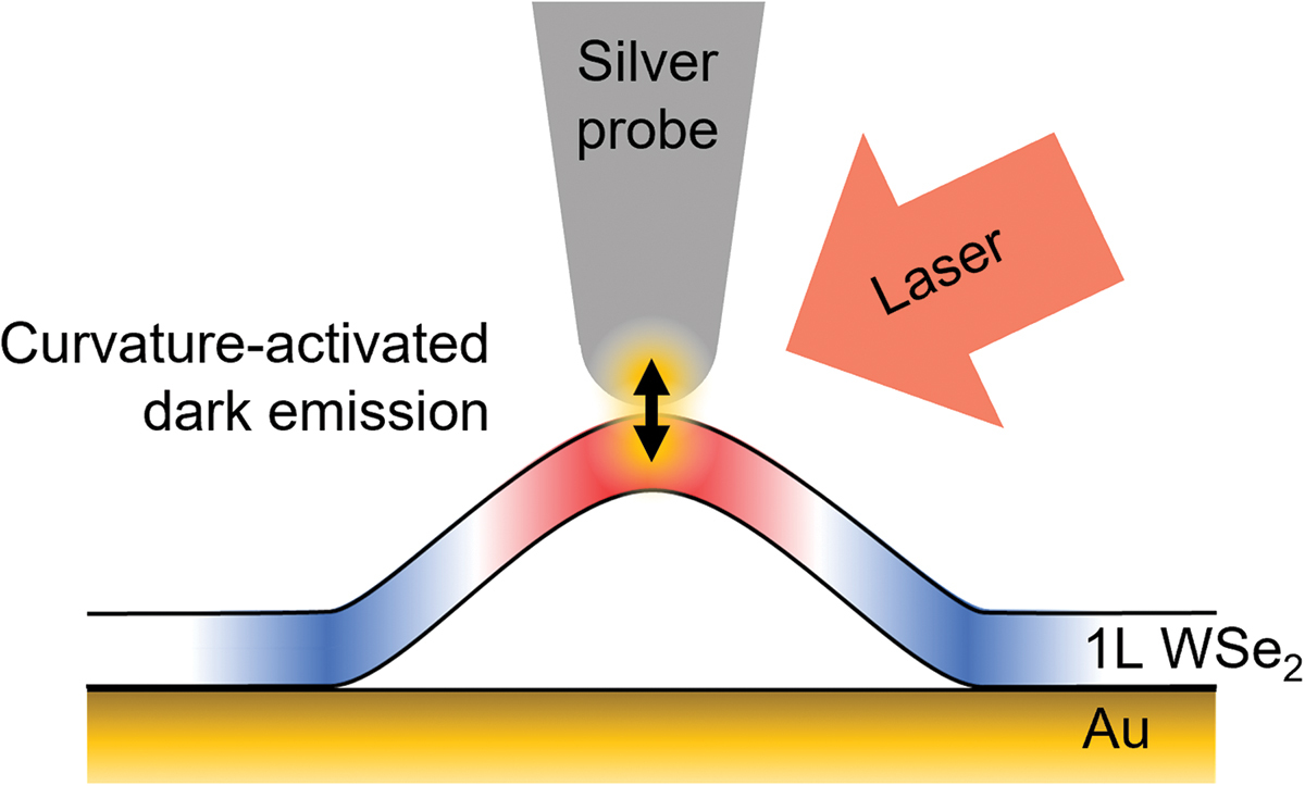 |
| Graphical abstract of the work. © Science and Technology of Advanced Materials) |
| The effects of stretching and bending are not always easy to distinguish, but by combining advanced measurement techniques, their results show that this alternative paradigm is a promising route towards room-temperature quantum light sources. |
| Curvature is much easy to engineer than stretching strain and so this result could accelerate progress towards low-cost quantum technologies. |
| NPL is currently working with groups in the UK and Brazil to do quantum chemical modelling and further experimental work to test the proposed paradigm and develop the theoretical understanding of how geometric curvature results in localised emission in monolayer tungsten diselenide. |
| Source: City University of Hong Kong (Note: Content may be edited for style and length) |

