| Posted: May 14, 2017 |
A silver molecular ink platform formulated for screen, inkjet, and aerosol jet printing(Nanowerk News) Researchers in Canada have demonstrated a screen-printable molecular ink that can be processed using both heat (thermal sintering) and light (photonic sintering) and can produce traces with submicron thicknesses and line widths as narrow as 41 µm. |
| The team has published their paper in ACS Applied Materials & Interfaces ("Versatile Molecular Silver Ink Platform for Printed Flexible Electronics"). |
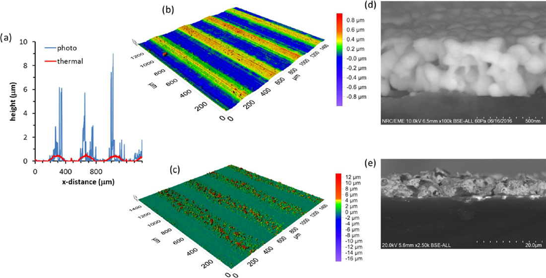 |
| Cross-sectional analysis of screen-printed lines (a), where the thermally sintered lines are relatively smooth (red line) in comparison to the photonically sintered traces (blue line). Representative surface profile images of screen-printed ∼200 µm wide traces after thermal (b, top right) and photonic sintering (c, bottom right) as well as a cross-sectional SEM image of the traces processed via thermal (d) and photonic sintering (e). (© ACS) (click on image to enlarge) |
| Printable electronics – an additive manufacturing technology – combines electronic materials with conventional printing processes to enable large-area, flexible, and/or low-cost manufacturing of membrane switches, thin film transistors (TFTs), and sensors as well as photovoltaics, antennas, and organic light-emitting diode (OLED)-based displays. |
| Conductive inks make up one of the largest markets in printed electronics as they enable the fabrication of key elements such as electrodes, antennas, and bus bars for current collectors using gravure, aerosol jet, inkjet or screen printing. |
| The printed electronics industry is driven, in part, by a desire to exploit additive manufacturing to reduce cost, and simply decreasing the silver content and the resulting trace thickness is an obvious means of achieving that goal. However, there are practical limitations in achieving high conductivity and mechanical robustness with flake-based inks because the traces require overlap of multiple layers of silver flakes and minimum thicknesses of ∼4 µm. |
| In their paper, the researchers present the development of a new class of screen-printable inks that make use of metal carboxylate salts as the silver metal precursor combined with a polymer binder to enable excellent screen printability, resolution, and mechanical properties of the conductive traces. |
| In addition, the silver molecular ink serves as a platform that can be easily tailored toward inkjet and aerosol jet printing to make low-resistivity traces (2x bulk) and TFT electrodes. Such a platform is not feasible with flake-based inks because of particle size limitations, leaving only relatively expensive nanoparticle inks as an alternative. |
| Despite the sub-micrometer thickness of the processed traces, the molecular ink can be printed on top of rough dielectric surfaces to produce functional metal-insulator-metal devices in a production environment. |
| Finally, the ink serves as a platform technology where all of the required components from the screen-printable ink can be incorporated into inks compatible with inkjet, aerosol spray, and screen printing, enabling many applications and devices (such as transistors) under development in printable electronics. |
 By
Michael
Berger
– Michael is author of four books by the Royal Society of Chemistry:
Nano-Society: Pushing the Boundaries of Technology (2009),
Nanotechnology: The Future is Tiny (2016),
Nanoengineering: The Skills and Tools Making Technology Invisible (2019), and
Waste not! How Nanotechnologies Can Increase Efficiencies Throughout Society (2025)
Copyright ©
Nanowerk LLC
By
Michael
Berger
– Michael is author of four books by the Royal Society of Chemistry:
Nano-Society: Pushing the Boundaries of Technology (2009),
Nanotechnology: The Future is Tiny (2016),
Nanoengineering: The Skills and Tools Making Technology Invisible (2019), and
Waste not! How Nanotechnologies Can Increase Efficiencies Throughout Society (2025)
Copyright ©
Nanowerk LLC
|
|
Subscribe to a free copy of one of our daily Nanowerk Newsletter Email Digests with a compilation of all of the day's news. |