| Posted: May 15, 2017 |
The ultimate tuning of optoelectric properties with nanoplatelets(Nanowerk News) An international research team has demonstrated an easy approach to synthesize ultrasmall near infrared 2D nanoplatelets (NIR NPLs) via template-assisted cation exchange. |
| The NPLs (PbSe or alloyed PbSe1–xSx) with lateral dimensions below 10 nm exhibit continuously tunable photoluminescence emission ranging from 1180 to 1380 nm thanks to the variation of the S/Se ratio, which cannot be achieved in binary NPLs, and a quantum yield of ∼60%, the highest reported for NIR NPLs so far. |
| They reported their findings in Advanced Energy Materials ("Ultrasmall Nanoplatelets: The Ultimate Tuning of Optoelectronic Properties"). |
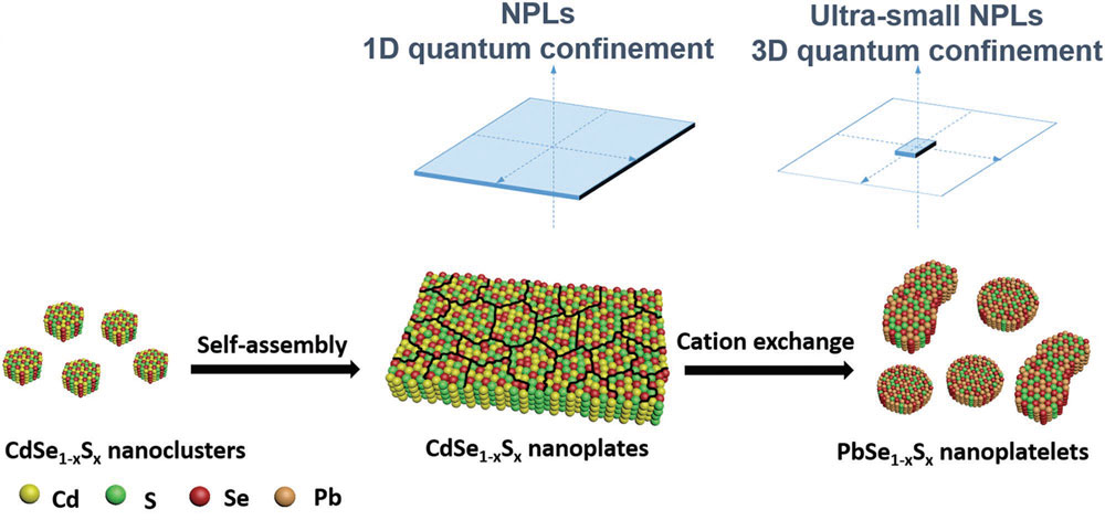 |
| Scheme of the formation of NIR NPLs through cation exchange using visible NPLs as template and 1D to 3D transition of quantum confinement from NPLs to ultrasmall NPLs. B,C,E–G) TEM bright-field images (BFI) of CdSe1–xSx NPLs (Se:S = 3:1). (© Wiley-VCH Verlag) (click on image to enlarge) |
| NPLs exhibit a series of outstanding optoelectronic properties for various applications in energy technologies, such as solar cells or solar-driven hydrogen production, because of their suitable electronic band structure for fast exciton dissociation, efficient charge transfer of photogenerated electron/hole pairs, and high photochemical stability. |
| Near infrared NPLs based on lead or tin chalcogenides enable a thickness-tunable wide absorption spectrum, ranging from ultraviolet to NIR, thereby matching the solar spectrum with significant overlap. |
| The authors write that theoretical simulations of the bandgap as a function of thickness, geometry, and size show that ultrasmall NPLs exhibit strong 3D quantum confinement, compared to 1D confinement in larger sized NPLs with similar thickness. |
| As a proof-of-concept, the team used the NPLs as photosensitizers for PEC hydrogen generation. After surface treatment with Cd, they obtained a saturated photocurrent density of ∼5 mA cm-2, nearly three times higher than the value obtained from PbS/CdS QDs under identical preparation and measurement conditions. |
 By
Michael
Berger
– Michael is author of four books by the Royal Society of Chemistry:
Nano-Society: Pushing the Boundaries of Technology (2009),
Nanotechnology: The Future is Tiny (2016),
Nanoengineering: The Skills and Tools Making Technology Invisible (2019), and
Waste not! How Nanotechnologies Can Increase Efficiencies Throughout Society (2025)
Copyright ©
Nanowerk LLC
By
Michael
Berger
– Michael is author of four books by the Royal Society of Chemistry:
Nano-Society: Pushing the Boundaries of Technology (2009),
Nanotechnology: The Future is Tiny (2016),
Nanoengineering: The Skills and Tools Making Technology Invisible (2019), and
Waste not! How Nanotechnologies Can Increase Efficiencies Throughout Society (2025)
Copyright ©
Nanowerk LLC
|
|
Subscribe to a free copy of one of our daily Nanowerk Newsletter Email Digests with a compilation of all of the day's news. |