| Posted: Jun 04, 2017 |
New microscopy technique for nanomechanical subsurface imaging(Nanowerk News) Researchers at Northwestern University report the development of scanning near-field thickness resonance acoustic microscopy (SNTRAM) – an imaging technology with sharp phase contrast and mechanical sensitivity that provides a wide range of applications in nanomechanical imaging of semiconductor structures and a wide range of other materials. |
| The findings have been reported in ACS Nano ("Thickness Resonance Acoustic Microscopy for Nanomechanical Subsurface Imaging"). |
| Acoustic waves can be used to measure several properties, such as the thickness, sound speed, acoustic impedance, density, bulk modulus, and attenuation, for a wide range of materials, soft as well as hard. |
| Since these are elastic strain waves that can travel through different materials, without any damage to them, they can be used for imaging subsurface structures noninvasively, a concept used widely in medical imaging. |
| Nanoscale spatial resolution can be achieved by combining atomic force microscopy (AFM) and ultrasonic microscopy, using an AFM probe as a local mechanical detector of elastic waves. |
| However, the combination of ultrasonics with AFM platform is still a developing area of research, where understanding the physics of the mechanism of detection and determining the sensitivity of detection of surface or subsurface properties are still in progress. |
| Despite the progress in ultrasonic-based methods, some of the major challenges are a) how better image contrast can be generated due to high signal-to-noise of the transmitted ultrasound wave to the other side of the sample; and b) the sensitive detection of the local variation in material properties at much better resolution due to a sharp change in phase (especially when two materials have similar mechanical properties). |
| In this newly developed SNTRAM technique, the sample is actuated at a frequency corresponding to the lowest longitudinal thickness resonance mode or resonance modes in the actuating transducer, and the AFM cantilever is operated in contact mode. The sample is resonating at its natural resonance frequency via the piezotransducer underneath it. |
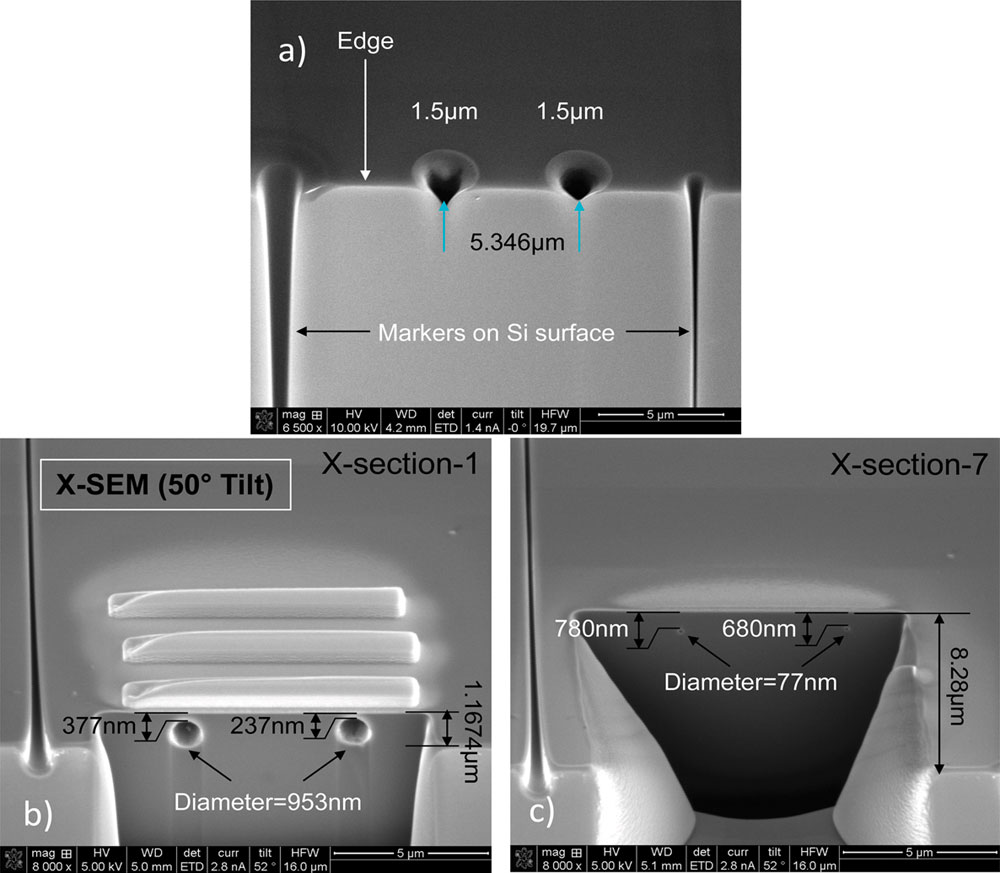 |
| (a) 1.5 µm size holes created with FIB etching, (b) cross-sectional SEM image at 50° tilt, and (c) holes with reduced diameter deep inside the bulk from both the edge and top surface. (© ACS) (click on image to enlarge) |
| The authors demonstrated the versatility of this technique by imaging buried conical holes created by FIB and low-K dielectrics patterned trenches. |
| We believe our development will fill a critical void in the subnanometer spatial range for nondestructive subsurface imaging in physical sciences. |
 By
Michael
Berger
– Michael is author of four books by the Royal Society of Chemistry:
Nano-Society: Pushing the Boundaries of Technology (2009),
Nanotechnology: The Future is Tiny (2016),
Nanoengineering: The Skills and Tools Making Technology Invisible (2019), and
Waste not! How Nanotechnologies Can Increase Efficiencies Throughout Society (2025)
Copyright ©
Nanowerk LLC
By
Michael
Berger
– Michael is author of four books by the Royal Society of Chemistry:
Nano-Society: Pushing the Boundaries of Technology (2009),
Nanotechnology: The Future is Tiny (2016),
Nanoengineering: The Skills and Tools Making Technology Invisible (2019), and
Waste not! How Nanotechnologies Can Increase Efficiencies Throughout Society (2025)
Copyright ©
Nanowerk LLC
|
|
Subscribe to a free copy of one of our daily Nanowerk Newsletter Email Digests with a compilation of all of the day's news. |