| Posted: Jun 29, 2017 |
Self-assembled quantum dot drives a plasmonic nanocircuit(Nanowerk News) Plasmonic nanocircuits have the potential to miniaturize integrated photonic circuits and bridge integrated electronics and photonics. |
| A research team in Germany has demonstrated a simple model quantum plasmonic nanocircuit with a narrow-band self-assembled GaAs quantum dot as a source for single plasmon excitation. |
| This work, reported in Nano Letters ("On-Chip Single-Plasmon Nanocircuit Driven by a Self-Assembled Quantum Dot"), addresses the problem of how to integrate self-assembled semiconductor quantum dots as single-photon sources in plasmonic nanocircuits by releasing the emitters from the bulk crystal and exploiting an indirect-coupling approach. |
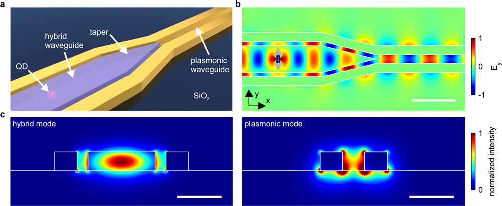 |
| Geometry of the structure and numerically simulated properties. (a) Schematic of the structure for efficient excitation of a plasmonic waveguide with a self-assembled quantum dot. (b) Instant distribution of Ey in the midplane of the structure when excited with a y-polarized dipole (light gray arrow) at the center of the waveguide, showing the propagating wave and mode conversion at the taper. The scale bar is 500 nm. (c) Profiles of the relevant modes of the hybrid waveguide (left) and the plasmonic waveguide (right). The electric-field intensity of each panel is normalized in such a way that both modes have the same power. The scale bars are 200 nm. The outlines of the structure are overlaid in (b,c). (© American Chemical Society) (click on image to enlarge) |
| On the basis of this approach, more complex plasmonic as well as photonic circuits can be developed. For example, multiple quantum dots can be coupled via plasmonic circuits to achieve photonic transistors. |
| By applying voltages on the gold wires, it may be possible to electrically tune the transitions of the quantum dots into resonance. |
| By using site-controlled self-assembled quantum dots, additional flexibility with device design can be obtained. |
| The authors point out that in situ lithography approaches using photoluminescence or cathodoluminescence or approaches of predetermination of the quantum dot position could also help to position quantum dots in devices. |
| Plasmonic components such as interferometers, modulators, and switches can be readily integrated due to the flexible EBL-based fabrication. |
| Moreover, electrical excitation of the quantum dot and electrical detection of single-plasmons can be implemented to make all-on-chip circuits. |
| "Semiconductors are well-developed materials for integrated electronic circuits and a wide variety of semiconductor-based quantum photonic circuits are being established as well," the authors conclude their report. "Our work shows that by making use of the self-assembled quantum dots, quantum plasmonic circuits can also be built on semiconductor platforms, and it thus opens the way to integrate electronic, photonic, and plasmonic devices on one semiconductor chip for applications of quantum technologies." |
 By
Michael
Berger
– Michael is author of four books by the Royal Society of Chemistry:
Nano-Society: Pushing the Boundaries of Technology (2009),
Nanotechnology: The Future is Tiny (2016),
Nanoengineering: The Skills and Tools Making Technology Invisible (2019), and
Waste not! How Nanotechnologies Can Increase Efficiencies Throughout Society (2025)
Copyright ©
Nanowerk LLC
By
Michael
Berger
– Michael is author of four books by the Royal Society of Chemistry:
Nano-Society: Pushing the Boundaries of Technology (2009),
Nanotechnology: The Future is Tiny (2016),
Nanoengineering: The Skills and Tools Making Technology Invisible (2019), and
Waste not! How Nanotechnologies Can Increase Efficiencies Throughout Society (2025)
Copyright ©
Nanowerk LLC
|
|
Subscribe to a free copy of one of our daily Nanowerk Newsletter Email Digests with a compilation of all of the day's news. |