| Posted: Aug 23, 2017 |
Stretchable metallic nanoclusters for wearable electronics(Nanowerk News) Researchers have fabricated highly deformable and stretchable conductors utilizing a Coil Flash Thermal Evaporation (CFTE) of gold nanoclusters that form robust thin metallic layers and maintain conductivity up to 200% on PDMS and 150% on textured rubber. |
| The CFTE method is known to produce gold nanoclusters with low ionization and kinetic energies, which minimizes carbonization of elastomers during deposition. |
| As the researchers report in ACS Applied Materials & Interfaces ("Facile Fabrication of Ultra-Stretchable Metallic Nanocluster Films for Wearable Electronics"), high metal-elastomer adhesion is obtained with textured substrates. |
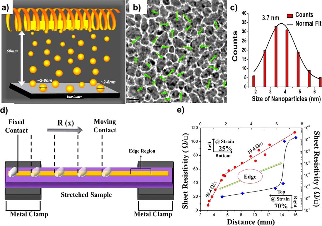 |
| (a) Schematics showing the formation of low energy gold nanoclusters incident on stretchable elastomers. (b) TEM image of the deposited nanoclusters during the early stages of cluster coalescence. The green arrows show some of the deposited nanoclusters having a grainy morphology on a background of coalesced clusters. Scale bar-20 nm (c) The size distribution of the metal nanoclusters is shown along with a Normal fit (average cluster size ∼3.7 nm). (d) Shows the setup with eutectic liquid alloy contacts used for measurements. The discontinuity regions and the method to map them is shown. (e) Shows the change in resistance R(x) along the sample length for 25% and 70% strained samples emphasizing the discontinuity effect. Axes: (25% Bottom-Left and 70% Top-Right). (© ACS) (click on image to enlarge) |
| The CFTE-gold films on textured substrates are highly robust and perform significantly better than e-beam, sputtered and implanted electrodes and exhibit only a small increase in resistance with strain (25 Ω-sq-1 at 100% strain). |
| The films stretch and relax in a bellow type open-and-close mechanism which allow for a robust performance with cyclic straining. |
| The CFTE is a one-step low vacuum process (0.5 × 10⁻² millibar), not requiring intensive fabrication setups and large processing durations associated with other vapor deposition based processes. |
| The authors point out that the facile nature of this process opens up possibilities for easy incorporation of these electrodes for various functionalities involving deformable electronics like textile electronics, biointerfacing of devices, lab-on-chip devices, robotics, and stretchable metallic interconnects. |
| "Low cost and high throughput should make it possible to easily facilitate the integration of this process into numerous industrial production lines and clean room fabrication setups for ubiquitous electronics," they conclude their report. |
 By
Michael
Berger
– Michael is author of four books by the Royal Society of Chemistry:
Nano-Society: Pushing the Boundaries of Technology (2009),
Nanotechnology: The Future is Tiny (2016),
Nanoengineering: The Skills and Tools Making Technology Invisible (2019), and
Waste not! How Nanotechnologies Can Increase Efficiencies Throughout Society (2025)
Copyright ©
Nanowerk LLC
By
Michael
Berger
– Michael is author of four books by the Royal Society of Chemistry:
Nano-Society: Pushing the Boundaries of Technology (2009),
Nanotechnology: The Future is Tiny (2016),
Nanoengineering: The Skills and Tools Making Technology Invisible (2019), and
Waste not! How Nanotechnologies Can Increase Efficiencies Throughout Society (2025)
Copyright ©
Nanowerk LLC
|
|
Subscribe to a free copy of one of our daily Nanowerk Newsletter Email Digests with a compilation of all of the day's news. |