| Nov 21, 2018 |
Atom-by-atom construction of an artificial molecule(Nanowerk News) In chemistry, the wave functions of electrons bound to nuclei determine the chemical characteristics of atomic and molecular species. In this context, an artificial molecule (AM) can be defined as a system whose local electronic structure has been engineered to emulate molecular electronic orbitals. |
| Coupled quantum dots as well as collections of superconducting circuits both meet this criterion and indeed have been referred to as AMs. |
| An alternative system that has also been described as an AM is based on colloidal particles arranged with various geometries and compositions but does not meet the criterion of producing a molecular electronic structure. |
| The colloidal particles do, however, demonstrate an aspect of real molecules that has not, to date, been reproduced by the other approaches: functionality derived from complex geometrical arrangement of constituent 'atoms'. |
| Hydrogen atoms on a silicon surface – H-Si (100) – behave as a resist that can be patterned with perfect atomic precision using a scanning tunneling microscope (STM). Such STM-based hydrogen lithography offers the flexibility necessary to create an atom-sized quantum dot in the form of a dangling bond deterministically at any lattice point in the 2D plane of the H-Si (100) surface. |
| In new work reported in Nano Letters ("Atom-by-Atom Construction of a Cyclic Artificial Molecule in Silicon"), researchers using hydrogen lithography have constructed an AM that both meets the electronic structure definition and demonstrates a nontrivial geometry: a cyclic atomic configuration spanning three dimer rows. |
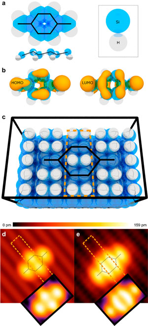 |
| Ring-structure Si-based molecule and analogous artificial molecule built by STM. (a) Top and side views of Si8H8 molecule in vacuum. Blue spheres represent Si atoms, and gray spheres represent hydrogen. A skeletal chemical structure is overlaid to aid in identification of corresponding features in subsequent images. The side view highlights that the molecule is not planar but rather has a chair conformation. (b) Calculated electron orbitals, HOMO and LUMO, of the molecular analogue. Orbitals are displayed as isosurfaces of the squared wave function. (c) Artificial molecule built on the passivated Si (100) surface by selective removal of H atoms. (d) STM constant current topography images of the occupied states, and (e) unoccupied states of the artificial molecule. Insets show the corresponding simulated images based on DFT calculations. The orange, dashed overlay in panels c-e indicates the location of the central dimer row in each, where a dimer is defined to be a pair of two covalently bonded surface Si atoms. Imaging conditions are -2 V sample bias and 30 pA current set point for panel d and +2 V sample bias and 30 pA current set point for panel e. Both images are 5 nm × 5 nm. (Reprinted with permission by American Chemical Society) |
|
"Our constructed AM has an electronic structure exhibiting strong similarity to that of the Si8H8 molecule and is artificial in both its construction from dangling bonds and its scale, which is larger by a factor of 2 in comparison to the equivalent gas-phase molecule," the autors write. "What is particularly interesting about the cyclic Si8H8 AM is that it exhibits delocalized |
| The scientists therefore expect that their AM can be used as a building block for artificial silicene devices of arbitrary shapes and sizes, with the interesting property that their honeycomb structure is twice the size of real silicene. |
| Another practical application is the use of AMs as designer potential wells for precision doping of silicon. More generally, AMs can generate desired chemical behavior on the Si surface localized to regions where the STM has patterned them. |
 By
Michael
Berger
– Michael is author of four books by the Royal Society of Chemistry:
Nano-Society: Pushing the Boundaries of Technology (2009),
Nanotechnology: The Future is Tiny (2016),
Nanoengineering: The Skills and Tools Making Technology Invisible (2019), and
Waste not! How Nanotechnologies Can Increase Efficiencies Throughout Society (2025)
Copyright ©
Nanowerk LLC
By
Michael
Berger
– Michael is author of four books by the Royal Society of Chemistry:
Nano-Society: Pushing the Boundaries of Technology (2009),
Nanotechnology: The Future is Tiny (2016),
Nanoengineering: The Skills and Tools Making Technology Invisible (2019), and
Waste not! How Nanotechnologies Can Increase Efficiencies Throughout Society (2025)
Copyright ©
Nanowerk LLC
|
|
Subscribe to a free copy of one of our daily Nanowerk Newsletter Email Digests with a compilation of all of the day's news. |