| Jul 25, 2011 |
Spintronics: A high wire act |
| (Nanowerk News) Graphene is a promising material for a wide range of applications due to its remarkable mechanical and electronic properties. An application of particular interest is spin-based electronics, or spintronics, in which the spin orientation of an electron is used to perform circuit functions in addition to its charge. Bongsoo Kim and colleagues from KAIST, Hanyang University and Samsung in Korea now report the integration of ferromagnetic nanowire arrays on graphene substrates, opening up a route for the construction of graphene-based spintronic devices using nanowires as spin-injecting contacts ("Epitaxially Integrating Ferromagnetic Fe1.3Ge Nanowire Arrays on Few-Layer Graphene"). |
| The spin of an electron is a property that, like charge, can be used to encode, process and transport information. However, spin information is easily lost in most media, which has made spintronics difficult to realize in practice. In graphene, on the other hand, spin can be preserved for longer due to its peculiar electron transport properties. "Low intrinsic spin–orbit coupling, long spin diffusion lengths and vanishing hyperfine interaction are features of graphene that make it a promising medium for spin transport," explains Kim. |
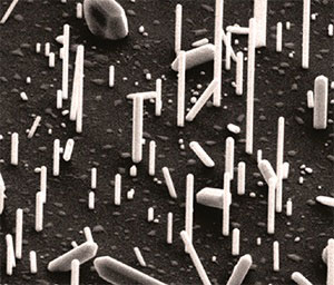 |
| Scanning electron microscopy image of vertical iron germanide nanowires grown on graphene. (© ACS 2011) |
| A prerequisite for the realization of spintronic devices based on graphene is its integration with ferromagnetic contacts to allow spin injection. Kim and his co-workers found that nanowires of iron germanide (Fe1.3Ge) serve as efficient contacts for this purpose. "Iron germanide nanowires show low resistivity and room-temperature ferromagnetism, and they are compatible with existing complementary metal–oxide–semiconductor technologies," says Kim. |
| To produce the atomically well-defined interfacial contact between the nanowires and the graphene surface needed for optimum device performance, the researchers deposited the contacts by an epitaxial method based on chemical vapor transport. Through careful adjustment of deposition parameters such as carrier gas flow rate and reaction temperature, the researchers produced vertically aligned nanowires that are closely lattice-matched to the graphene sheets (see image). |
| Initially preparing the graphene sheets on a substrate of silicon oxide allowed the researchers to isolate the final nanowire–graphene structure by etching and then transfer it to another substrate, greatly expanding the versatility of the approach. It is a delicate process, however. "It is necessary to transfer the graphene films onto the substrate very carefully in order to avoid folding and wrinkling of the graphene," says Kim. |
| Source: Tokyo Institute of Technology |

