| Posted: April 7, 2008 |
Winning nanotechnology images from the Science as Art competition |
| (Nanowerk News) The 2008 MRS Spring Meeting concluded in San Francisco on March 28. As a special feature of the meeting, the MRS conducted the fifth installment of the popular "Science as Art" competition. (View winners from past competitions). The competition was open to all meeting attendees, with entries on display in the Moscone West Convention Center. Here are the six first-place and second-place awards: |
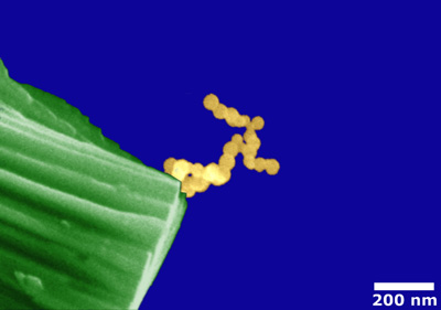 |
| Jumper Sometimes the thesis just gets to be too much... This image is of some contamination (probably monodisperse polystyrene spheres from a previous user) in the microscope which just happened to collect at the corner of a Ta2O5 particle. The image was collected using secondary electrons in a Hitachi S-4700 SEM and was colorized using the Gnu Image Manipulation Program (GIMP). (Image: Georff Brennecka, Sandia National Laboratories) |
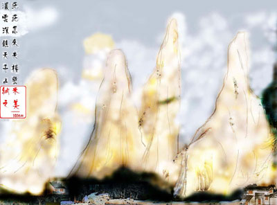 |
| Chinese painting This image was color-added from one ZnO nanoneedle SEM image. The nanoneedles look like beautiful mountains in a Chinese painting. (Image: Hui Ying Yang, Nanyang Technological University, Singapore) |
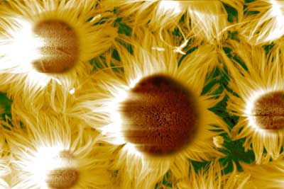 |
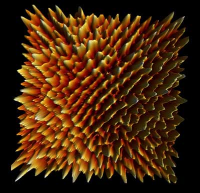
| Field of Sunflowers Amorphous SiOx nanowire bundles have an uncanny ability to self-assemble into various shapes, including one that strikingly resembles a sunflower. In these sunflowers, highly packed bundles form the disc florets and loosely packed ones around the rim of the disc form the ray florets. The scanning electron image shows a field of sunflowers. The grey-scale image was mapped into pseudo-colors by graphic software. The nanowires grew out of the reaction of Si and oxygen, with molten Ga and Au acting as catalysts. Each nanowire is about 10 nm in diameter and tens of micrometers in length. (Image: S.K. Hark, The Chinese University of Hong Kong) |
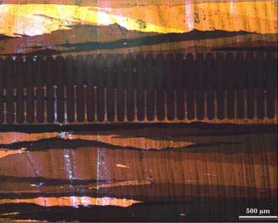 |
| Landscape painting This is a cross-polarized light optical microphotograph of an array of organic thin-film transistors (OTFT) fabricated with newly synthesized, highly crystalline 4T-TMS organic semiconductor deposited by newly developed solution-shearing method. Besides the excellent performances these new OTFTs exhibited, this microphotograph represents itself an aesthetic landscape painting full of beauty and art— different parts of the cross polarized thin film look like lakes, lands, mountains and sunglows, while the gold electrodes of the transistors seem to be a fence between lakes and far-away mountains... (Image: Zihong Liu, Stanford University) |
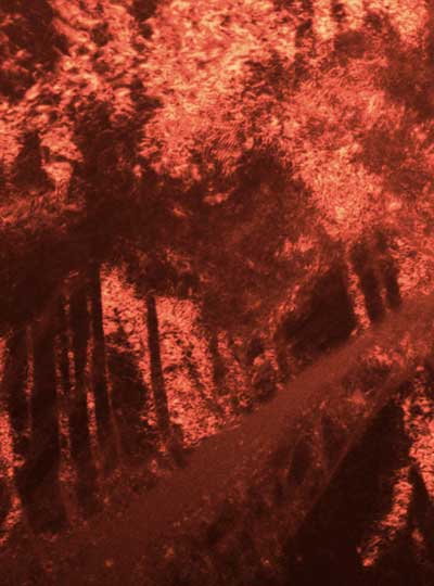 |
| Inferno Color-enhanced TEM micrograph showing twins and strain contrast in a post-compression [111] NiTi micropillar. The micropillar was produced via FIB milling and was compressed using a nanoindenter equipped with a flat punch. By creating and testing compression pillars in a range of diameters, this method allows us to study the effect of size scale on the shape memory behavior of NiTi. (Image: Blythe Gore Clarkk, Max-Planck-Institut für Metallforschung) |
 |
| Big Bang AFM image of a sputtered Au(001) single crystal. (Image: Violeta Navarro, Universidad Complutense de Madrid) |
We have a collection of these amazing images in some of our articles on Nanowerk. You can find them here:
| Source: MRS |

