| Nov 09, 2017 |
New method developed to 3-D print fully functional electronic circuits
|
|
(Nanowerk News) Researchers at the University of Nottingham have pioneered a breakthrough method to rapidly 3D print fully functional electronic circuits.
|
|
The circuits, which contain electrically-conductive metallic inks and insulating polymeric inks, can now be produced in a single inkjet printing process where a UV light rapidly solidifies the inks.
|
|
The breakthrough technique paves the way for the electronics manufacturing industry to produce fully functional components such as 3D antennae and fully printed sensors from multiple materials including metals and plastics.
|
|
The new method combines 2D printed electronics with Additive Manufacturing (AM) or 3D printing - which is based on layer-by-layer deposition of materials to create 3D products. This expands the impact of Multifunctional Additive Manufacturing (MFAM), which involves printing multiple materials in a single additive manufacturing system to create components that have broader functionalities.
|
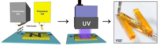 |
| A schematic diagram showing how UV irradiation heats and solidifies conductive and dielectric inks to form the letter N with silver tracks that connect a green LED to a power source. (Image: University of Nottingham)
|
|
The new method overcomes some of the challenges in manufacturing fully functional devices that contain plastic and metal components in complex structures, where different methods are required to solidify each material.
|
|
Existing systems typically use just one material which limits the functionality of the printed structures. Having two materials like a conductor and an insulator, expands the range of functions in electronics. For example, a wristband which includes a pressure sensor and wireless communication circuitry could be 3D printed and customised for the wearer in a single process.
|
|
The breakthrough speeds up the solidification process of the conductive inks to less than a minute per layer. Previously, this process took much longer to be completed using conventional heat sources such as ovens and hot plates, making it impractical when hundreds of layers are needed to form an object. In addition, the production of electronic circuits and devices is limited by current manufacturing methods that restrict both the form and potentially the performance of these systems.
|
|
Professor Chris Tuck, Professor of Materials Engineering and lead investigator of the study, highlighted the potential of the breakthrough, 'Being able to 3D print conductive and dielectric materials (electrical insulators) in a single structure with the high precision that inkjet printing offers, will enable the fabrication of fully customised electronic components. You don't have to select standard values for capacitors when you design a circuit, you just set the value and the printer will produce the component for you.'
|
|
Professor Richard Hague, Director of the Centre for Additive Manufacturing (CfAM) added, 'Printing fully functional devices that contain multiple materials in complex, 3D structures is now a reality. This breakthrough has significant potential to be the enabling manufacturing technique for 21st century products and devices that will have the potential to create a significant impact on both the industry and the public.'
|
How it works
|
|
Dr Ehab Saleh and members of the team from CfAM found that silver nanoparticles in conductive inks are capable of absorbing UV light efficiently. The absorbed UV energy is converted into heat, which evaporates the solvents of the conductive ink and fuses the silver nanoparticles. This process affects only the conductive ink and thus, does not damage any adjacent printed polymers. The researchers used the same compact, low cost LED-based UV light to convert polymeric inks into solids in the same printing process to form multi-material 3D structures. A video showing how the concept works is available here
|
|
With advancements in technology, inkjet printing can deposit of a wide range of functional inks with a spectrum of properties. It is used in biology, tissue bioprinting, multienzyme inkjet printing and various types of cell printing, where the 'ink' can comprise of living cells.
|
|
The breakthrough has established an underpinning technology which has potential for growth in academia and industry. The project has led to several collaborations to develop medical devices, radio frequency shielding surfaces and novel structures for harvesting solar energy.
|

