| Dec 02, 2019 |
Taking 3D printing of electronic parts to the next level
|
|
(Nanowerk News) The rise of additive manufacturing – or as it's more commonly known, 3D printing – has enabled the rapid production of complex parts across many domains. As the techniques have become more refined, the semiconductor industry has taken note. But until recently, no one's been able to form single-crystal materials – the building block of semiconductors – with traditional additive manufacturing processes.
|
|
That's about to change. Researchers at the Johns Hopkins Applied Physics Laboratory (APL), in Laurel, Maryland, have demonstrated a novel and groundbreaking way to additively print gallium nitride (GaN) — a material that can be used to produce semiconductor power devices as well as radio-frequency components and light-emitting diodes – using a combination of liquid and gas.
|
|
Their work was detailed in the journal MRS Communications ("A pathway to compound semiconductor additive manufacturing").
|
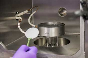 |
| A sapphire wafer being loaded it into the reactive additive material chamber for gallium nitride printing. (Image: Johns Hopkins University Applied Physics Laboratory)
|
|
"Gallium nitride is a material of significant interest for optoelectronic applications, solar power generation and high power distribution," said Jarod Gagnon, a materials scientist in APL’s Research and Exploratory Development Department and lead author on the paper. "Being able to 3D-print semiconductors gives us the ability to make complex devices that are either too costly or too complex to make with current techniques. If we're successful with our research, this will open a new path forward for a rapid change in how we operate in the semiconductor and electronic device field."
|
|
GaN printing represents a new category of 3D printing that Gagnon and his colleagues refer to as "gas-phase reactive AM." Building off of work completed under a 2018 Combustion Grant, the team combined additive manufacturing techniques – in this case, material extrusion – with semiconductor synthesis techniques (liquid phase epitaxy and metalorganic chemical vapor deposition) to react with the material as it's printed. "This is what allowed us to form single-crystal oriented material through epitaxial growth," he explained.
|
|
The team is the first to report on this concept; Gagnon attributes the scarcity of research to a disconnect between the two fields of additive manufacturing and semiconductor synthesis. All of the additive manufacturing techniques — vat polymerization, material jetting, binder jetting, material extrusion, power bed fusion, sheet lamination and directed energy deposition — result in polycrystalline materials limiting the application space of that work.
|
|
"I approached this problem from a semiconductor viewpoint instead and realized that we could modify and combine existing processes in both research areas to create something new and effective," he said. "That isn't to say it wasn't still a difficult challenge. Additive manufacturing processes and semiconductor processes both have a wide number of critical variables that affect the quality of the final product. Now that we've proven the viability of our process, we have double the number of variables that interrelate and have to be controlled and understood to demonstrate the ultimate quality and resolution of our process."
|
|
The requirements for the process, in terms of controlling impurities and safety, were so novel that the team – which includes Michael Presley, Nam Le, Timothy Montalbano and Steven Storck – had to design and build a system that would allow them to perform the research, creating a new capability at APL in the process.
|
|
"We believe this capability will be useful for exploratory efforts into additive manufacturing of other material systems that have been relegated to the 'this isn't going to work' pile," Gagnon said.
|
|
The team is now looking for ways to improve the resolution of the printing process and better understand the mechanisms at play using modelling and experimental efforts.
|
|
"We have a lot of unanswered questions for this process," Gagnon said. "It's a different way of doing things than anyone has done before, which means we have a lot of catch-up to do in terms of our fundamental understanding of this process. But we are constantly thinking about what other material systems this process may be useful for, because this new process and system has the potential to open even more doors in the future."
|

