| May 13, 2013 |
Conversion efficiency of 10.5% for thin-film microcrystalline silicon solar cells
|
|
(Nanowerk News) Hitoshi Sai (Senior Researcher), Advanced Low Cost Processing Team, the Research Center for Photovoltaic Technologies of the National Institute of Advanced Industrial Science and Technology (AIST), has developed a novel light-trapping structure to enhance optical absorption inside thin-film silicon solar cells, in collaboration with the Photovoltaic Power Generation Technology Research Association (PVTEC). A conversion efficiency of 10.5% – the highest ever for thin-film microcrystalline silicon solar cells – has been achieved by using the developed light-trapping structure.
|
|
Unlike the conventional light-scattering structures with irregularity, the developed light-trapping structure has a periodic structure with holes a few micrometers in diameter arranged in a honeycomb pattern (a honeycomb texture). The researchers were able to understand the relationship between the shape and size of this periodic light-trapping structure and the characteristics of the solar cells. On the basis of this relationship, a high short-circuit current density was obtained by optimizing the honeycomb texture and improving the doping layer and the transparent conductive film.
|
|
The results indicate that using a highly controlled light-trapping structure can effectively enhance optical absorption inside solar cells. By optimizing the design of the structure and applying it to multi-junction solar cells, further improvement in the performance and conversion efficiency of the solar cells is expected.
|
|
Details of this technology was presented at the 60th Japan Society of Applied Physics Spring Meeting to be held from March 27 to 30, 2013 at the Kanagawa Institute of Technology in Atsugi, Kanagawa Prefecture and at the Materials Research Society Spring Meeting to be held from April 1 to 5, 2013 (PDT) in San Francisco, U.S.A.
|
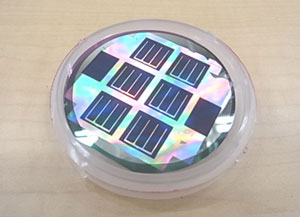 |
| A microcrystalline silicon solar cell formed on a honeycomb-textured substrate. A microcrystalline silicon solar cell (5 cm in diameter) formed on a honeycomb-textured substrate.
|
|
Social Background of Research
|
|
In recent years, the popularization of solar cells as one of renewable energy sources has been promoted actively. Most commercialized solar cells are crystalline silicon solar cells. Further cost reduction is required to promote the popularization of solar cells, while solar cells integrated with building materials are being developed to create a new market.
|
|
Because a silicon thin film less than a few micrometer thick is used as the power-generating layer, thin-film silicon solar cells are largely free from resource constraints and can be fabricated on large substrates by using plasma-assisted chemical vapor deposition, making it easy to reduce costs through mass production. Because an integrated series-connection structure, which is hard to create for crystalline silicon solar cells, can be formed, thin-film silicone solar cells can be easily applied to building materials. However, for widespread use, the conversion efficiency of thin-film silicon solar cells must be increased: it is currently as low as half of that of crystalline silicon solar cells.
|
|
To effectively use sunlight energy distributed over a wide range of wavelengths, most of the current thin-film silicon solar cells are multi-junction solar cells in which an amorphous silicon solar cell to generate power from visible light and a microcrystalline silicon solar cell to generate power from visible to near-infrared light are stacked monolithically. The conversion efficiency of each type of solar cell needs to be increased to improve the conversion efficiency of these multi-junction solar cells.
|
|
History of Research
|
|
AIST has been conducting research and development to improve the performance of thin-film silicon solar cells. For microcrystalline silicon solar cells, it has developed a high-pressure depletion method that can achieve both high-speed film forming and high conversion efficiency in collaboration with Mitsubishi Heavy Industries Ltd., and in recent years it has been conducting the research in a light-trapping structure.
|
|
PVTEC has set up the PVTEC Tsukuba Laboratory at AIST as a research center aiming at the rapid commercialization of next-generation solar cells and has been conducting research and development to improve performance – particularly of large-area thin-film solar cells.
|
|
One of the technical issues concerning the improvement in the conversion efficiency of microcrystalline silicon solar cells is the need to enhance light-absorbing ability. In the present research, AIST and PVTEC have worked together to develop a light-trapping technology to achieve sufficient light absorption in the power-generating layer.
|
|
The present research was conducted as part of "Research and Development of Solar Energy Technology: Development of Next-generation High-performance Technology for Photovoltaic Power Generation System – Research and Development of Next-generation Multi-junction Thin Film Silicon Solar Cells through Industry–Academia–Government Collaboration (FY2010 – 2015)" commissioned by the New Energy Development Organization. Part of this research was conducted at the Nanoprocessing Facility with the support of IBEC Innovation Platform of AIST.
|
|
Details of Research
|
|
In microcrystalline silicon solar cells, a thin film composed of tiny grains of crystalline silicon, which has a low absorption coefficient in the infrared region, is used as a power-generating layer. Therefore, technology for trapping light in the power-generating layer and achieving sufficient light absorption is required to increase the conversion efficiency. Until now, technology has been used that forms a textured structure with micro-irregularities 0.1 to 10 micrometers in size on the substrate; the light-scattering thus produced increases the effective optical path length in the power-generating layer, thereby enhancing light absorption. However, if a silicon thin film is formed on a steep texture, defects are created in the film, resulting in deterioration of the power-generation characteristics. Because of this, if an excessively textured structure is used, the conversion efficiency does not increase even though the light absorption increases. An irregular structure produced naturally during the formation of a transparent conductive film or a metal electrode thin film is used in most of the textured light-trapping structures in thin-film silicon solar cells. However, because the shape and size of the textured structure is limited by the film-forming conditions and the irregularity occurs in the structure, the relationship between the shape and size of the textured structure and the characteristics of solar cells is not well understood. No clear guidelines have therefore been established for improving the performance of thin-film silicon solar cells.
|
|
To solve these issues, the researchers fabricated various types of well-controlled light-trapping structures using photolithography and then used the light-trapping structures to fabricate microcrystalline silicon solar cells. Evaluation of the solar cells revealed the relationship between structural parameters and solar cell characteristics. The newly developed light-trapping structure has a honeycomb texture with holes several micrometers in diameter arranged in a honeycomb pattern as shown in Fig. 1. The diameter and the depth of the holes can be controlled independently. As a result, the relationship between solar cell characteristics and a wide range of shapes and sizes of textured structure was understood. Because of the regularity of the structure, dispersion due to irregularity was eliminated and the effect of the shape and size of the structure on solar cell characteristics can be understood more clearly.
|
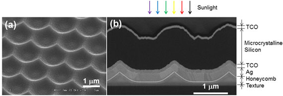 |
| Figure 1: (a): Surface profile of the honeycomb-textured structure. (b) Cross-section of the thin-film microcrystalline silicon solar cell with honeycomb-textured structure.
|
|
It was found that because the structural parameters of the honeycomb-textured structure that provides the highest conversion efficiency depend on the film thickness of the solar cell, the light-trapping structure needs to be designed to suit the film thickness. It was also found that deterioration of power generation due to the textured structure can be minimized by selecting an appropriate shape and size. The researchers obtained a very high short-circuit current density for thin-film silicon solar cells by using the optimum honeycomb-textured structure fabricated on the basis of the results, together with a highly transparent doping layer and a transparent conductive oxide thin film developed by AIST. They have also increased the conversion efficiency of thin-film microcrystalline silicon solar cells from 10.1% (the highest value so far) to 10.5% (Fig. 2A). This suggests that the power-generation characteristics can be further improved by changing the basic design of the light-trapping structure. The conversion efficiency of solar cells depends on the product of open-circuit voltage (VOC), short-circuit current density (JSC), and fill factor (F.F.). In the developed solar cell, the short-circuit current has been substantially improved, but the VOC value of 0.521 V and the F.F. value of 71.6% are lower than the reported values (VOC = 0.539 V, F.F. = 76.6%). The conversion efficiency is expected to be further increased by improving these values.
|
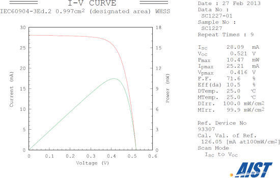 |
| Figure 2: Power-generation characteristics of the developed microcrystalline silicon solar cell. The efficiency of the solar cell is evaluated by an independent organization as official data. In the graph, the red line shows the current–voltage characteristics and the green line shows the output power–voltage characteristics, with the peak indicating the maximum output power. VOC, F.F., and ISC are the open-circuit voltage, fill factor, and short-circuit current, respectively. The short-circuit current density (JSC) is obtained by dividing ISC by the device area. The conversion efficiency, Eff (da), is the product of VOC, F.F., and JSC. The measurements were taken by Characterization and Standardization Team of the Research Center for Photovoltaic Technologies, AIST. This team has been researching and developing technologies for high-precision measurement of the performance of solar cells. The team conducts internationally consistent, neutral and high-precision evaluations of the performance of various types of solar cell, including current–voltage characteristics, and is comparable to the National Renewable Energy Laboratory in the United States and the Fraunhofer Institute for Solar Energy Systems in Germany.
|
|
Future Plans
|
|
In this research, the researchers have improved the efficiency of microcrystalline silicon solar cells. Most types of thin-film silicon solar cells have a multi-junction structure, and the light absorption capacity of all of the solar cells that make up this structure needs to be enhanced to increase the conversion efficiency. The researchers intend to further increase the efficiency by applying the new light-trapping structure to multi-junction solar cells. They also intend to develop a technology for applying the results to large-area solar cells so as to realize low-cost solar cells.
|

