| Jun 26, 2012 |
Structurally flexible silicene integrated with Si wafers
|
|
(Nanowerk News) As the Si counterpart of graphene, “silicene” is an atom-thick, ultimately thin, two-dimensional crystal of silicon. A team of researchers at the Japan Advanced Institute of Science and Technology (JAIST), Antoine Fleurence, Rainer Friedlein, Taisuke Ozaki, and Yukiko Yamada-Takamura, has succeeded in preparing silicene on Si wafers via a ceramic zirconium diboride buffer layer, paving the way for an integration of silicene with existing Si-based technologies that intrinsically face limits with top-down approaches. Most importantly, while this is (almost) impossible for the rather rigid graphene, whose development led to the 2010 Nobel Prize in Physics, it has been found that a direct band gap can be induced in silicene by structural control. The presence of a band gap is essential for the use of silicene in electronic devices that perform logical operations.
|
|
While, already in 1994, Japanese researchers theoretically studied the stable structure of silicene, experimental evidence for its existence has been scarce so far. With a combination of experimental techniques, such as scanning tunneling microscopy and photoelectron spectroscopy, also carried out at the Photon Factory Synchrotron Radiation Facility (KEK, in Tsukuba, Japan), and supported by first-principles calculations, the JAIST team verified the intimate relationship between the structure of epitaxial silicene and the resulting electronic properties.
With its tunable electronic properties and foreseeable integration into existing Si-based technologies, one may expect silicene to challenge the dominance of graphene in nanoscale physics and in technological applications.
The results of this research are being published in Physical Review Letters ("Experimental Evidence for Epitaxial Silicene on Diboride Thin Films")
|
|
This research has been supported by KEK, Funding Program for Next Generation World-Leading Researchers (NEXT Program) by the Japan Society for the Promotion of Science (JSPS) and KAKENHI.
|
|
Background
|
|
Graphene and silicene are both atom-thick honeycomb sheets of a single element with four valence electrons, carbon (C) and silicon (Si), respectively (Fig. 1). The element Si is the larger cousin of C in the periodic table. While the Nobel-Prize awarded creation of graphene presents the hottest playground for physics and nanotechnology so far, until recently, it was thought to be impossible to form similar sheets of Si atoms. This is because the four valence electrons prefer to hybridize in a different way than C atoms, in the so-called sp3 hybridization instead of the sp2 hybridization. The creation of silicene by our team on the thin film of conductive ceramic called zirconium diboride (ZrB2) and independently by French researchers on a different platform, surfaces of silver single crystal, came therefore as a surprise.
|
|
For silicene, the electronic structure and a large number of astonishing electronic and transport properties like the presence of very light and mobile charge carriers are predicted to be similar to those in graphene if the same crystal structure is adopted. However, silicene may also have distinctively different electronic properties since it is more stable in a number of slightly-buckled forms while graphene is perfectly planar. Buckling means that neighboring Si atoms are displaced out of the plane. Silicene may therefore also occur with a variety of lattice constants, and also with tunable electronic properties related to a different degree of buckling.
|
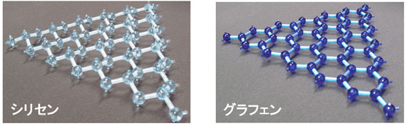 |
| Figure 1: Stick-and-ball models of silicene and graphene.
|
|
Experimental
|
|
Our silicene is spontaneously formed under ultrahigh vacuum (UHV) conditions and at high temperatures on thin films of a conductive ceramic called ZrB2 that are grown with a good lattice matching (“epitaxially”) on Si(111) wafers. These diboride films are grown at high temperatures by thermal decomposition of zirconium borohydride gas on wafers cut in size of approximately 10 x 20 mm2. When the as-grown ZrB2 film is cooled to room temperature, silicene has already formed. That is, Si atoms diffuse from the Si wafer to the diboride film surface to form silicene in a spontaneous way. In our study, the structural and electronic properties of silicene have been characterized by scanning tunneling microscopy (STM) (Fig. 2) and photoelectron spectroscopy, both in home laboratories and at the Photon Factory synchrotron radiation facility, part of the High-Energy Accelerator Research Organization (KEK), located in Tsukuba, Japan. In order to achieve better understanding of the experimental results, first-principles calculations of the crystal and electronic structures of epitaxial silicene were carried out.
|
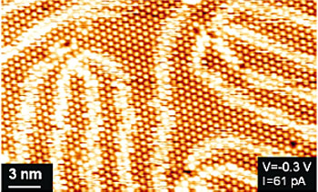 |
| Figure 2: STM image of silicene on ZrB2 thin film.
|
|
Main Results
|
|
1. Reproducible formation of silicene on Si wafers via buffer layers
|
|
The experimental data provide clear proof for the presence of two-dimensional, epitaxial silicene with -electronic states and thus for at least partial sp2 hybridization. Moreover, silicene and diboride film surfaces, which were oxidized upon exposure to air, were restored by just heating at approximately 800? under UHV condition. In this method, Si atoms forming silicene are supplied from the Si wafer underneath the ZrB2 film. An atom thick silicene is formed uniformly and spontaneously. The reproducibility of silicene preparation using this method is therefore much better as compared to techniques involving the evaporation of Si on substrates.
|
|
2. Possible tuning of electronic structure using epitaxy
|
|
We demonstrate that the particular buckling leads to a direct band gap for silicene-derived electronic states. The presence of a band gap may allow the use in electronic devices that perform logical operations, and the presence of a direct band gap may allow the use also in optical devices. Our silicene is so far the only crystalline allotrope of silicon with this important property. Since the buckling is determined by the contact to the substrate (see, Fig.3), the results imply that the atomistic structure and thus the electronic properties can be changed by the choice of appropriate substrates with selected lattice parameters. This highlights the advantage of structurally flexible silicene compared to rather rigid graphene in which it is difficult to introduce a band gap.
|
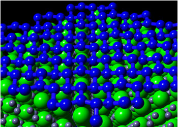 |
| Figure 3: The result of theoretical calculation of a stable silicene structure on ZrB2(0001).
|
|
Future Prospects
|
|
The growth with a good lattice matching on large-scale silicon wafers via diboride buffer layers provides already a way to integrate silicene into existing Si-based technologies that intrinsically face limits with top-down approaches. Once it would be created on an insulating platform, silicene with its tunable electronic properties may challenge the dominance of graphene in nanoscale physics and technological applications. In particular, while (almost) impossible for the rather rigid graphene, the creation of a direct band gap by structural control is essential for optoelectronic and transistor applications, and thus for any device performing logical operations.
|

