| Apr 01, 2014 |
Printed Electronics Europe 2014 award winners
|
|
(Nanowerk News) Printed, flexible and organic electronics will eventually impact most aspects of human endeavour, with the enabling materials, equipment, components and manufacturing being developed and launched today. To recognize and award outstanding achievement to those involved in this rapidly growing business the annual IDTechEx Printed Electronics Awards are held each year. The annual awards were announced at the annual IDTechEx Printed Electronics event this week in Berlin, Germany - Europe's leading event on the topic that brings together end users with suppliers..
|
|
The entries were judged by the following experts panel:
|
|
– Professor Dr.-Ing. Gunter Hübner , Hochschule der Medien, Germany
– Professor Iain McCulloch, Imperial College, UK
– Professor Gyoujin Cho, Sunchon National University, Korea
|
|
A summary of the awards and winners are as follows:
|
|
Academic R&D Award - Fraunhofer IFAM
Best Technical Development Materials Award - VTT
Best Technical Development Manufacturing Award (Sponsored by NovaCentrix) - Suzhou institute of Nanotech
Best Product Development Award - ISORG / PLASTIC LOGIC
Best Commercialization Award - BlueSpark / Iontera
|
|
Academic R&D Award - Fraunhofer IFAM
|
|
Fraunhofer Institute for Manufacturing Technology and Advanced Materials (IFAM) won this award for the development of a thermoelectric energy generation (TEG) device manufactured by digital printing. Thermoelectric devices harvest energy from heat gradients which can be used to power devices such sensor networks and electric microsystems. Printing them enables simpler production with a path to high volume manufacturing.
|
|
Using a self-prepared Copper, Nickel and Magnesium alloy ink and a commercial silver ink TEG structures were deposited at Fraunhofer IFAM on different surfaces using printing technologies. A fully inkjet-printed TEG on a ceramic substrate is shown in the figure.
|
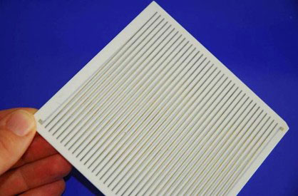 |
| Fully Inkjet-printed TEG structure on ceramic substrate. (Source: Fraunhofer IFAM)
|
|
The temperature gradient of ΔT = 100 K results in a converted electrical voltage of U ∼ 80 mV and a current of I ∼ 60 nA, respectively. Due to the fact, that the resulting power is relatively low and only sufficient for the operation of ultra-low-power applications, further investigations will enhance structural thickness to reduce the TEG overall electrical resistance. Furthermore thermoelectric power will be increased by using nano-composite materials showing high electrical conductivity in coexistence with low thermal conductivity. These materials promise high ZT-values and can also be adapted to digital printing techniques. Nevertheless the fully printed TEGs allow an application on almost any surface combined with a resource efficient production due to usage of printing technologies and an environmental friendly use of thermoelectric polymers and composites.
|
|
Best Technical Development Materials Award - VTT
|
|
VTT won this award for developing a new process for synthesis of metallic nanoparticles based on gas-phase reduction of metal chloride precursors. The aim of this project is to scale up the synthesis from laboratory to the pilot scale capable of daily production of 200-2000 g/d of metallic nanopowders.
|
|
The objective of the pilot unit TIPU is to demonstrate economical and sustainable production of nanoparticles.
The targeted production costs for the metallic nanopowders is in the order of 100 €/kg. The reactor allows
continuous week long operation, where pure metal powders are produced in one-step process starting from
inexpensive precursor materials. The process is energy efficient and operating in atmospheric pressure, which
directly influence the investment costs of the facility. The pilot unit TIPU is constructed using refractory materials
commonly applied in the industry. In addition, the facility consumes very little water and produces minimal
amount of liquid waste.
|
|
Best Technical Development Manufacturing Award (Sponsored by NovaCentrix) - Suzhou institute of Nanotech
|
|
The touch panel industry has experienced unprecedented rapid growth in the last few years. While ITO is still dominant in this sector for making the transparent conductive film (TCF), which is the key material for a touch panel, its many drawbacks have stimulated widespread R&D activities to find alternative materials to replace it.
|
|
Researchers at Suzhou Institute of Nanotech, Chinese Academy of Sciences, have developed a novel approach to making the metal meshes for TCF. By embedding nanosilver ink into high resolution trenches on a PET substrate, TCFs with mesh lines less than 2µm in width, sheet resistance less than 1 ohm per square and haze less than 1.5% have been achieved. Another important feature is its simplicity in manufacturing touch panels. Coating conductive material, patterning touch electrodes and printing bezels can all be done in a single roll-to-roll process. The technology has been implemented at O-film Inc., China, in high volume manufacturing and touch panels based on the new TCFs have adopted by major domestic and international brands of tablet and notebook computers manufacturers.
|
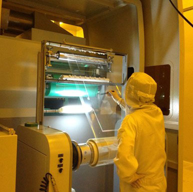 |
| Photo of roll-to-roll manufacturing of metal mesh transparent conductive film. (Image: Suzhou Institute of Nanotech)
|
|
Best Product Development Award - ISORG/PLASTIC LOGIC
|
|
ISORG and Plastic Logic have worked together to bring new applications to market with an image sensor on plastic.
|
|
The collaboration is based on the deposition of organic printed photodetectors, pioneered by ISORG, onto a plastic organic thin-film transistor backplane, developed by Plastic Logic, to create a flexible sensor with a 4x4 cm active area, 375µm pitch (175µm pixel size with 200µm spacing) and 94 x 95 = 8930 pixel resolution.
|
|
The transistor backplane technology originally developed by Plastic Logic for e-readers can be used in a sensor array : instead of writing voltage onto voltage capacitors, the same pixels are used to store charge created by the organic photodetector layer, and the charge is read off, row by row, to read the image. Organic electronics will offer similar opto-electronic performances to silicon image sensors but many more functionalities for new product design.
|
|
This collaboration demonstrates the versatility of organic electronics to combine two different technologies to create new and disruptive products for a broad range of markets. The first large area image sensor on plastic has already attracted strong interest from industry and consumer electronics leaders for new applications and functionalities.
|
|
Best Commercialization Award - BlueSpark / Iontera
|
|
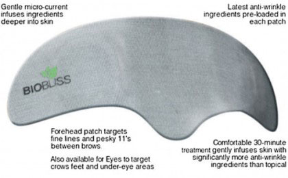
BlueSpark and Iontera won this award for the successful commercialisation of the Biobliss patch - a skincare product that can be used in conjunction with current skin care regimens. With proven clinical safety and efficacy in reducing the appearance of fine lines and wrinkles, Biobliss users have been amazed by the results reducing wrinkles on the forehead and the crow's feet area around the eyes. While traditional wrinkle creams simply sit on the surface of your skin, requiring hours of wear time for absorption to occur, the Biobliss Patch operates using a micro-current process, that gently pushes dermatologist-approved anti-wrinkle ingredients to the surface of the skin.
|
|
The Biobliss patch micro-current process is made possible through the use of conductive and printed materials along with Blue Spark's thin, flexible, printed battery technology. Both the printed materials and Blue Spark's printed batteries utilize high volume, roll-to-roll screen-printing processes for efficient manufacturing. The net result is a thin, flexible, disposable, micro-current delivery mechanism that conforms to the skin and is soft to the touch.
|
 |
|
Biobliss was launched in March 2013 in specialty spas and dermatology offices. Following on that success, the product was picked up by high end US retailers Bergdorf Goodman and Nieman Marcus. In January 2014 the product debuted to critical success on the Home Shopping Network TV outlet, selling out the forehead product in one hour. Biobliss is on Track to be distributed by two additional major US retailers by mid 2014. Patches can also be ordered directly from the Biobliss website, www.biobliss.com
|
|
The next IDTechEx Printed Electronics awards will be held at the USA event, in Santa Clara, CA, USA on November 19-20, 2014. For more details see www.PrintedElectronicsUSA.com
|
|
Printed Electronics Asia will be held in Tokyo, Japan, on Sept 1-5. See www.PrintedElectronicsAsia.com for more details.
|

