| Posted: Nov 30, 2006 |
Focused ion beam milling of nanocavities could lead to photon-on-demand light sources |
| (Nanowerk Spotlight) Artificial opals are gemstones that are of considerable scientific and technological interest as photonic crystals, as components of light sources, solar cells, and chemical sensors. They are conveniently made from periodic stackings of nanospheres. It would be exciting if one could fabricate optical cavities in these photonic crystals by removing, or adding high dielectric material to a single unit cell in the structure. These optical cavities would localize light that potentially enables the fabrication of high-resolution miniature on-chip sensors, or even qubits for quantum computers. Previously, such controlled modification of the nanostructure of a single colloid in an opal has not been achieved. Now, researchers in The Netherlands developed a method for realizing both single and arrays of material cavities, or defects, in individual colloids on the surface of silicon dioxide artificial opals by a focused ion beam milling technique. This research could ultimately lead to the fabrication of a photon-on-demand light source. |
| There are basically two possible routes for obtaining individual modified particles in opals. The first route is modifying individual particles and moving them to their desired position on the opal. Moving and placing such particles with nanometer precision is quite challenging and requires the use of, e.g., robots or atomic force microscopes. The second route is modifying a single colloid a posteriori in an already grown artificial opal. |
| "The essence of our work is that we are able to control the shape of individually addressed nanoparticles inside artificial opals" Léon Woldering explains to Nanowerk. "To this end, we fabricate nanocavities in individual colloidal particles. We can change the position of these cavities at will, and also tune the diameter of these structures with nanometer precision. We thus realize a kind of nano-donut, or nano-bead. We are able to make these tiny cavities by means of focused ion beams. Not only is the nanotechnology to make these cavities extremely interesting in itself but also the method we developed to mill these structures on a non-conducting substrate is novel and expands the possibilities of focused ion beam milling in general." |
| Woldering is a member of the Complex Photonic Systems group (COPS) in the Faculty of Science and Technology at the University of Twente in The Netherlands. |
| In a recent paper ("Focused ion beam milling of nanocavities in single colloidal particles and self-assembled opals"), Woldering and colleagues from COPS, MESA+ Institute for Nanotechnology and FOM Institute for Atomic and Molecular Physics describe a versatile method for modifying the structure of targeted individual silicon dioxide colloidal particles on the surface of opals with controllable features with radii smaller than 40 nm using focused ion beam milling (FIB). Circularly shaped material cavities, and even arrays of cavities, were milled in the colloids, converting the particles into donut-like or bead-like structures. |
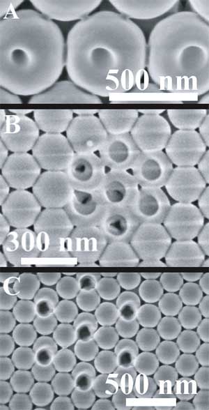 |
| (A) Scanning electron micrograph of three colloidal spheres on the surface of an artificial opal of silicon dioxide colloidal spheres. The spheres are milled intermittently with a 50 x 50 nm2 square pattern. The left sphere was milled for 5 s, the middle sphere was milled for 10s (2 x 5s) and the right sphere for 15 s (3 x 5s). (B) Scanning electron micrograph of an array of seven milled material cavities on the surface of an artificial opal of silicon dioxide colloidal spheres. The defects on this sample were milled in parallel for a total of 1.2 s in four sweeps of 300 ms each, using a circular pattern with a radius of 60 nm. (C) Scanning electron micrograph of a different array of seven milled material cavities on the surface of an artificial opal of silicon dioxide colloidal spheres. The defects on this sample were milled in parallel for a total of 6.3 s, using a circular pattern with a radius of 60 nm. The pattern was displaced with respect to the centers of the spheres and the defects were milled between two spheres. (Reprinted with permission from IOP Publishing) |
| "Our motivation is the fabrication of an optical cavity in a 3-dimensional photonic crystal by adding additional opal layers to the structures we fabricated, and subsequent inversion of the crystal" Woldering explains. "The inverse opal will be a silicon, or a titanium dioxide structure. In order to study the confinement of light we plan to probe the emission from quantum dots placed near, or inside the optical cavity. Alternatively, if the crystal surrounding a cavity in which light is confined is switched by modifying the refractive index, we may be able to release the confined photon at will. This will allow the fabrication of a photon-on-demand light source." |
| The research of the Dutch scientists has significant potential, and several exciting opportunities arise if the shape and morphology of individual particles can be controlled, for three reasons: |
| 1) The technique will allow the fabrication of optical cavities in photonic crystals made by self-assembly of colloids. |
| 2) Alternatively, if a monolayer of nanospheres is used as a lithographic opal mask, the nano-donuts can act as additional apertures in the mask of which size and shape can be modified. |
| 3) Modified colloids can also be used as size-selective moieties in chemically active substrates. |
| Woldering points out that the biggest challenge the researchers are facing at the moment is the question "How we will be able to find the nanocavities, once they are inside the bulk, covered with additional opal layers?", which is the next step in their research. |
| "By fabricating nanocavities in artificial opals and subsequently hiding them in the middle of a 3D structure we have fabricated a true 'needle-in-a-haystack' that will require some creativity to be solved" says Woldering. "Fortunately, we think we have already nearly developed tricks to solve this issue." |
| The COPS group is also doing some extensive research in the emission of quantum dots in photonic crystals. Using quantum dots, they were the first ever to control emission from light sources in a photonic environment, an effect first predicted by Eli Yablonovitch in 1987. This result was published in Nature back in 2004 ("Controlling the dynamics of spontaneous emission from quantum dots by photonic crystals"). |
| Of similar interest is the group's research on all-optical ultrafast switching of silicon photonic crystals. Ultrafast switching is the prerequisite in the photon-on-demand concept. See for example "All-optical ultrafast switching of Si woodpile photonic band gap crystals" and "Spatial homogeneity of optically switched semiconductor photonic crystals and of bulk semiconductors". |
 By
Michael
Berger
– Michael is author of four books by the Royal Society of Chemistry:
Nano-Society: Pushing the Boundaries of Technology (2009),
Nanotechnology: The Future is Tiny (2016),
Nanoengineering: The Skills and Tools Making Technology Invisible (2019), and
Waste not! How Nanotechnologies Can Increase Efficiencies Throughout Society (2025)
Copyright ©
Nanowerk LLC
By
Michael
Berger
– Michael is author of four books by the Royal Society of Chemistry:
Nano-Society: Pushing the Boundaries of Technology (2009),
Nanotechnology: The Future is Tiny (2016),
Nanoengineering: The Skills and Tools Making Technology Invisible (2019), and
Waste not! How Nanotechnologies Can Increase Efficiencies Throughout Society (2025)
Copyright ©
Nanowerk LLC
|

Become a Spotlight guest author! Join our large and growing group of guest contributors. Have you just published a scientific paper or have other exciting developments to share with the nanotechnology community? Here is how to publish on nanowerk.com.
