| Posted: Jun 30, 2009 |
Nanotechnology PacMan cuts straight graphene edges |
| (Nanowerk Spotlight) Graphene has two distinct types of edges produced when it is cut – armchair type or zigzag type – which correspond to the two crystal axis of graphene. These edge types are predicted theoretically to have distinct electronic, magnetic, and chemical properties, but current fabrication methods have no way of controlling which type of edge is produced and are dominated by disorder. For example, a common method is to use plasma etching which is an isotropic etching process and is not selective in which crystallographic direction it etches. This is a problem in especially nanoelectronics applications and devices (see for instance: Next generation nanotechnology computer memory made of graphene) where the potential performance of the device depends strongly on the edge structure as well. |
| A solution to this problem has now been found. Nanotechnology researchers have demonstrated anisotropic etching in single-layer graphene which produces connected graphene nanostructures with crystallographically oriented edges. This opens many future avenues to study graphene nanostructures such as nanoribbons, nanoconstrictions, and quantum dots with crystallographic edges. |
| "Our method is the first demonstration of an anisotropic etching process in graphene, which allows etching in a single crystallographic direction," Pablo Jarillo-Herrero tells Nanowerk. "Our work was motivated by the studies of graphite gasification by nickel. These studies date back decades to when it was observed that nickel nanoparticles would chew across a graphite surface, often eating along the crystal axis of the graphite. More recently, other groups have revisited this process under the new context of graphene and the exciting prospects of graphene nanostructures. It was natural then to try the same process in single layer graphene, which is after all a single atom thick layer of graphite." |
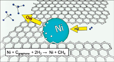 |
| Cartoon of a nickel (Ni) particle etching a graphene sheet (not to scale). Ni nanoparticles absorb carbon from graphene edges which then reacts with hydrogen (H2) to create methane. (Inset) Summary of the hydrogenation reaction that drives the etching process. (Reprinted with permission from American Chemical Society) |
| Jarillo-Herrero is an assistant professor of physics at MIT. Together with his group and collaborators from the Universidade Federal de Minas Gerais in Belo Horizonte and the Universidade de São Paulo, both Brazil, he discovered that in single layer graphene this nickel nanoparticle etching had an even more pronounced behavior than in graphite. |
| The team found that with their technique – anisotropic etching of single-layer graphene by thermally activated nickel nanoparticles – the cuts were running along a single crystallographic axis (in graphite cuts are produced in both of graphene's two crystallographic directions) and that they were uniformly small in size. |
| "Another important and mysterious behavior we observed in single-layer graphene etching was an effect whereby nickel nanoparticles while cutting across graphene would 'feel' the presence of another cut in front of it and turn away before crossing or coming in contact with the other trench," says Jarillo-Herrero. |
| The researchers reported their findings in the June 15, 2009 online edition of Nano Letters (Anisotropic Etching and Nanoribbon Formation in Single-Layer Graphene). |
| For the etching process, nickel nanoparticles produced on the surface of the graphene are heated up to high temperatures under hydrogen flow and then start chewing away the graphene like "Pacman", moving along crystallographic directions. A more scientific explanation is that the nickel nanoparticles etch the graphene through catalytic hydrogenation of carbon, where carbon atoms from exposed graphene edges dissociate into the nickel nanoparticle, and then react with hydrogen at the nickel surface. |
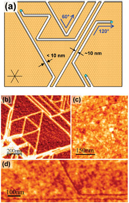 |
| Nanoparticle-assisted etching in single-layer graphene. Key features of etching in single-layer graphene are chirality-preserving angles of 60° and 120°, avoided crossing of trenches leaving ∼10 nm spacing between adjacent trenches and producing connected nanostructures, and trenches and nanoparticles with uniform width <10 nm. (b) AFM phase image of etched single-layer graphene with produced geometric nanostructures. The phase image obscures small details, making adjacent trenches appear to merge together. (c) AFM height image of equilateral triangle connected to three nanoribbons. (d) AFM height image of a trench which avoids crossing another trench, running parallel to it. (Reprinted with permission from American Chemical Society) |
| Jarillo-Herrero points out that his team's method demonstrates etching along a single crystallographic direction of graphene, which corresponds to a single type of edge. "Using our method it should be possible to experimentally demonstrate the unique properties of a graphene nanostructure due a special edge type." |
| Currently, though, the scientists do not control where the nanoparticles begin etching – they are randomly distributed on the edge of the graphene when the etching process begins. Also, it would be desirable for all the nanoparticles to run parallel to each other in a single absolute direction producing an array of nanoribbons and other predetermined structures. |
| The most immediate application for this technique is for producing graphene nanostructures which could be used for electronic devices such as field effect transistors (FET). |
| "Graphene nanostrucutures such as nanoribbons are interesting because they produce a band gap in the normally zero-gap graphene," explains Jarillo-Herrero. "A band gap is necessary for effective field effect transistor operation and would result in a transistor which would take advantage of the excellent electrical properties of graphene. Since our nanostructures have oriented edges, we predict that they would have better performance then current graphene FETs which have disordered edges." |
| He continues to explain that graphene nanostructures have interesting chemical properties which could make them useful for chemical sensors: "Graphene already is very sensitive to its environment because it is a surface, there is no bulk which is shielded from the outside. Graphene is especially reactive at its edges and by controlling the edge structure with methods such as ours it may be possible to produce devices with electrical properties dependent on molecules attached to the graphene's edges." |
| This new etching method also works on free standing graphene membranes or 'suspended graphene'. Graphene membranes are very strong and are impermeable to atoms as small as helium. Such membranes could see applications as support membranes for Transmission Electron Microscopes or have biological applications as membranes for nanopores as well. The ability to selectively etch such a membrane with nickel nanoparticles could bring the above mentioned electronic and chemical effects to the realm of graphene membranes as well. |
| Much of the early research on graphene focused on its electronic properties and applications. Increasingly now, graphene also grabs the interest of chemists, material scientists and even biologists. Although the bulk of today's graphene research still centers on nanoelectronics, it is the breadth of impact and applications which will grant graphene its staying power. The immediate challenge graphene research is faced with remains the issue of wide-scale, high-quality production of graphene material, as well as the precisely controlled fabrication of nanodevices. The above technique is a step towards overcoming this challenge. |
 By
Michael
Berger
– Michael is author of four books by the Royal Society of Chemistry:
Nano-Society: Pushing the Boundaries of Technology (2009),
Nanotechnology: The Future is Tiny (2016),
Nanoengineering: The Skills and Tools Making Technology Invisible (2019), and
Waste not! How Nanotechnologies Can Increase Efficiencies Throughout Society (2025)
Copyright ©
Nanowerk LLC
By
Michael
Berger
– Michael is author of four books by the Royal Society of Chemistry:
Nano-Society: Pushing the Boundaries of Technology (2009),
Nanotechnology: The Future is Tiny (2016),
Nanoengineering: The Skills and Tools Making Technology Invisible (2019), and
Waste not! How Nanotechnologies Can Increase Efficiencies Throughout Society (2025)
Copyright ©
Nanowerk LLC
|

Become a Spotlight guest author! Join our large and growing group of guest contributors. Have you just published a scientific paper or have other exciting developments to share with the nanotechnology community? Here is how to publish on nanowerk.com. |
