| Posted: Dec 14, 2006 |
Rewritable multi-component photonic circuits |
| (Nanowerk Spotlight) Along the way to all-optical devices in communication and information technology, photonic crystals play a significant role. They form a basis material for the future realization of optical components and circuits, and maybe even complex optical circuits or optical computers. Examples include complex waveguides, integrated microcavities, channel drop filters, optical switches and low-threshold lasers. All such devices depend on the inclusion of defect structures, non-linear materials and/or light-emitters into photonic bandgap material. |
| The combination of several devices into one photonic crystal would allow to realize the optical equivalent of an electronic circuit. So far, the intentional inclusion of such combined structures was very difficult to realize in practice, however. A group of German and Italian researchers now present a powerful technique that allows to create such photonic circuits inside photonic crystals by controlled micro-infiltration of liquid substances with sub-micron resolution. This approach forms an enabling technology for the realization of all optical devices and circuits. |
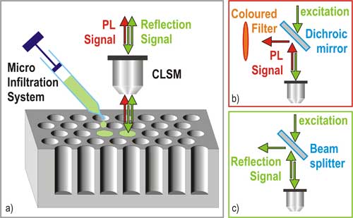 |
| Principle of the infiltration technique. Controlled infiltration is accomplished by a micro infiltration system that can be positioned with 100 nm accuracy and monitored with a scanning near-field microscope and confocal microscope. The infiltration system has femto-liter precision and can be used with a wide variety of liquids and suspensions. (Image: Dr. Wiersma) |
| "With our technique it is possible to address and infiltrate each pore of a two-dimensional photonic crystal individually with a liquid of specific refractive index and non-linear constant, and/or with a local light source" Dr. Diederik Wiersma explains to Nanowerk. |
| Wiersma is a researcher in the Optics of Complex Systems group at the European Laboratory for Non-linear Spectroscopy (LENS), the largest interdisciplinary laser laboratory in Italy and part of a European network of large scale laser facilities. |
| Wiersma and his colleagues reported their findings, titled "Rewritable photonic circuits" in the November 20, 2006 edition of Applied Physics Letters. |
| The researchers chose to infiltrate a solution of water and the organic dye Rhodamine 6G. The chemical and physical properties of this solution appear particularly appealing for the proposed approach. The basis material in which to perform the infiltration is periodic two-dimensional macroporous silicon which has been shown to behave as high quality twodimensional photonic crystal. The silicon pore walls were all covered with a thin silicon oxide layer to allow wetting of the pores. |
| "Note that the infiltration experiments are not restricted to this material and can be transferred to any other system with the appropriate wetting properties" says Wiersma. |
| The described technology can be applied to realize photonic circuits in two-dimensional photonic crystals. Since each pore of the photonic crystal can be addressed individually, different materials can be combined to write complex photonic circuits containing waveguides, active elements and sources. |
| Having demonstrated the feasibility of the technique, the researchers realized various structures. The images below show the results for an "S4 waveguide," obtained by reiterating a building block of four infiltrated pores organized in a bended geometry. |
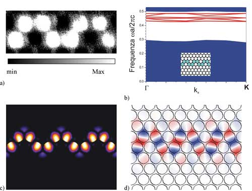 |
| (a) The luminescence signal from the infiltrated pores is shown. (b) The calculated band diagram for the TE modes associated with this structure. The blue regions correspond to propagating modes in the bulk crystal and the white region corresponds to the photonic band gap. The S4 waveguide introduces a miniband of guided modes red curves in the band gap. As shown in (c) and (d) the electromagnetic field associated with these modes is completely confined in the waveguide, demonstrating that the linear defect, introduced by the local infiltration of water, gives rise to an S-shaped waveguide in which light can propagate without losses at the sharp bends. (Image: Dr. Wiersma) |
| "Our technique enables the design and realization of various components and, above all, to combine several components into one single circuit"says Wiersma. "Another unique feature is that one can write both permanent structures and circuits that can be erased and rewritten." |
| Wiersma also points out that beyond its main application in integrated optics, the technique can be applied for any local infiltration application, e.g. to realize sensor chips by locally infiltrating a liquid that changes its optical properties when exposed to gas or biological species. |
| "Our research interest lies in the fundamental physics of light transport in complex photonic materials like photonic crystals and random lasers" says Wiersma. "The advantage of concentrating on fundamental research is that one often finds new applications that were unexpected and maybe even not predictable beforehand. Our latest infiltration technology, for instance, will give us an unprecedented flexibility in the realization of complex photonic devices and circuits." |
 By
Michael
Berger
– Michael is author of four books by the Royal Society of Chemistry:
Nano-Society: Pushing the Boundaries of Technology (2009),
Nanotechnology: The Future is Tiny (2016),
Nanoengineering: The Skills and Tools Making Technology Invisible (2019), and
Waste not! How Nanotechnologies Can Increase Efficiencies Throughout Society (2025)
Copyright ©
Nanowerk LLC
By
Michael
Berger
– Michael is author of four books by the Royal Society of Chemistry:
Nano-Society: Pushing the Boundaries of Technology (2009),
Nanotechnology: The Future is Tiny (2016),
Nanoengineering: The Skills and Tools Making Technology Invisible (2019), and
Waste not! How Nanotechnologies Can Increase Efficiencies Throughout Society (2025)
Copyright ©
Nanowerk LLC
|

Become a Spotlight guest author! Join our large and growing group of guest contributors. Have you just published a scientific paper or have other exciting developments to share with the nanotechnology community? Here is how to publish on nanowerk.com.
