| Posted: Aug 18, 2009 |
DNA nanotechnology in computers knocks down another roadblock |
| (Nanowerk Spotlight) DNA origami, tiny shapes and patterns self-assembled from DNA, have been heralded as a potential breakthrough for the creation of nanoscale circuits and devices. One roadblock to their use has been that they are made in solution, and they stick randomly to surfaces – like a deck of playing cards thrown onto a floor. Random arrangements of DNA origami are not very useful – if they carry electronic circuits for example, they are difficult to find and 'wire-up' into larger circuits. A collaboration between Caltech and IBM research Almaden has found a way to position and orient DNA origami on surfaces by creating sticky patches in the shape of origami – as a demonstration they positioned and aligned triangular DNA origami on triangular sticky patches. This success knocks down one of the major roadblocks for the use of DNA origami in computer nanotechnology. |
| Reporting their work in the August 16, 2009 online edition of Nature Nanotechnology (Placement and orientation of individual DNA shapes on lithographically patterned surfaces), the scientists demonstrate a way to put DNA origami exactly where they want it on a surface, to line them up like little ducks in a row. They do this by using electron-beam lithography, to make sticky patches that have the same shape as the outline of the DNA origami. |
| DNA origami is a method for folding long strands of DNA into whatever very small shape or pattern you desire. Using a computer-aided design program a scientist can design the desired nanoscale shape (typically about 100 nanometers across) and the computer designs a set of short DNA strands that can be ordered from a company that specializes in synthesizing DNA strands. The short DNA strands get mixed with the long DNA strands, heated up to nearly boiling, and cooled to room temperature over the course of a couple hours. In a single drop of water one then has 100 billion copies of the desired shape, or shape with a pattern on top. In the first DNA origami made were shapes like triangles and smiley faces, and patterns like maps of the western hemisphere, snowflakes, etc. |
| "The interesting thing about DNA origami is that it allows you to make such nanoscale shapes and patterns by pure self-assembly, Paul W. K. Rothemund explains to Nanowerk. "It gives you the power to place little tiny things, whether they are nanometer-sized electronic components or chemical entities into arbitrary arrangements without touching them or using some other man-made machine." |
| Rothemund, a senior research associate at Caltech, has been conducting groundbreaking research on using DNA origami to develop bottom-up nanotechnology fabrication techniques. Read his 2006 Nature paper Folding DNA to create nanoscale shapes and patterns or a more recent paper on bottom-up construction approaches ("DNA origami seeds to direct bottom-up fabrication processes"). |
| One problem today with DNA origami structures is that they are created in saltwater solution and they adhere randomly to surfaces, which means that "if you just pour DNA origami over a surface to which they stick, they attach everywhere," says Rothemund. "It's a little like taking a deck of playing cards and throwing it on the floor; they are scattered willy-nilly all over the place. Such random arrangements of DNA origami are not very useful. If they carry electronic circuits, for example, they are difficult to find and wire up into larger circuits." |
| Typically, though, nanoelectronics researchers would like their devices to be on a surface, like a silicon wafer, so that they can wire them up and integrate them with other technologies. "If the origami carry a device, you have to go find them, with some kind of ultramicroscopy like TEM or AFM, and then you have to use the very finest lithography we have to write special fine wires to them" says Rothemund. "It kind of defeats the purpose of using self-assembly in the first place." |
| In Rothemund's new work, conducted with a 10-strong research team at IBM's Almaden Research Center, led by Gregory M. Wallraff, the scientists used sticky patches of triangular DNA origami shape. |
| In a process developed by IBM scientists, electron-beam lithography and oxygen plasma etching, conventional semiconductor techniques, are used to make patterns on silicon wafers, creating lithographic templates of the proper size and shape to match those of individual triangular DNA origami structures created by Rothemund. The etched patches are negatively charged, as are DNA origami structures, and are therefore 'sticky'. |
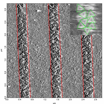 |
| IBM scientists are using DNA scaffolding origami to build tiny circuit boards; in this image, low concentrations of triangular DNA origami are binding to wide lines on a lithographically patterned surface. |
| To connect the origami to the templates, magnesium ions are added to the saltwater solution containing the origami. The positively charged magnesium ions can stick to both the DNA origami and the negatively charged patches on the template. Thus, when the solution is poured over the template, a negative-positive-negative 'sandwich' is formed, with the magnesium atoms acting as a glue to hold the origami to the sticky patches. |
| "So not only can we put origami where we want them, but they can be oriented in the direction we want them" Rothemund points out. |
| The positioned DNA nanostructures can then serve as scaffolds or miniature circuit boards for the precise assembly of components such as carbon nanotubes, nanowires, and nanoparticles at dimensions significantly smaller than possible with conventional semiconductor fabrication techniques. This opens up the possibility of creating functional devices that can be integrated into larger structures as well as enabling studies of arrays of nanostructures with known coordinates. |
| "The spacing between the components can be 6 nanometers, so the resolution of the process is roughly 10 times higher than the process we currently use to make computer chips," says Rothemund. "Then, if you want to design a really small electronic device, say, you just design DNA strands to create the pattern you want, attach little chemical 'fastening posts' to those DNA strands, assemble the pattern, and then assemble the components onto the pattern," he explains. |
| Further development of the technique is at the top of the team's to-do list. First will be new shapes that go down with an absolute orientation. "Triangles are symmetric and while we can orient them and control the direction they point, we can't control which of the three tip of the triangle points which way, or whether they go upside down or not," says Rothemund. "Making asymmetric shapes that line up and all point 'north' will be important. So to will be making multiple shapes that can all be used at once without interfering with each other so we can construct more complex patterns on surfaces." |
| The researchers pint out that there are still several roadblocks before we can see the use of DNA origami in computers – even after the 'placement and orientation problem' has been solved. For example, what is the best material to act as an electronic component on DNA origami? Should one use silicon nanowires, carbon nanotubes, graphene, gold nanocrystals, what? How can they be stuck to the origami in the highest yield with the best results? |
| "It really is difficult to say how long the remaining roadblocks will take –at least 5 years, more likely at least 10" says Rothemund. "But the solution to the current problem came much faster than expected." |
 By
Michael
Berger
– Michael is author of four books by the Royal Society of Chemistry:
Nano-Society: Pushing the Boundaries of Technology (2009),
Nanotechnology: The Future is Tiny (2016),
Nanoengineering: The Skills and Tools Making Technology Invisible (2019), and
Waste not! How Nanotechnologies Can Increase Efficiencies Throughout Society (2025)
Copyright ©
Nanowerk LLC
By
Michael
Berger
– Michael is author of four books by the Royal Society of Chemistry:
Nano-Society: Pushing the Boundaries of Technology (2009),
Nanotechnology: The Future is Tiny (2016),
Nanoengineering: The Skills and Tools Making Technology Invisible (2019), and
Waste not! How Nanotechnologies Can Increase Efficiencies Throughout Society (2025)
Copyright ©
Nanowerk LLC
|

Become a Spotlight guest author! Join our large and growing group of guest contributors. Have you just published a scientific paper or have other exciting developments to share with the nanotechnology community? Here is how to publish on nanowerk.com. |
