| Posted: Feb 15, 2010 |
Achieving ultralow nanoscale wear of one atom per micrometer |
| (Nanowerk Spotlight) Friction is the force that opposes the relative motion or tendency of such motion of two surfaces in contact. Historically, Leonardo da Vinci (1452-1519) was the first to enunciate two laws of friction. According to da Vinci, the frictional resistance was the same for two different objects of the same weight but making contacts over different widths and lengths. He also observed that the force needed to overcome friction is doubled when the weight is doubled. Similar observations were made by Charles-Augustin de Coulomb (1736-1806). The first reliable test on frictional wear was carried out by Charles Hatchett (1760- 1820) using a simple reciprocating machine to evaluate wear on gold coins. He found that compared to self-mated coins, coins with grits between them wore at a faster rate. The development of this branch of science, today called tribology is the science and technology of friction, lubrication, and wear, derived from the Greek tribo meaning "I rub". The new field of nanotribology extends the study of friction and wear processes on to nanometer scale. |
| Many nanotechnology applications are plagued by very poor wear resistance of device components at the nanoscale. Gears, bearings, and liquid lubricants can reduce friction in the macroscopic world, but the origins of friction for small devices such as micro- or nanoelectromechanical systems require other solutions. Despite the unprecedented accuracy by which these devices are nowadays designed and fabricated, their enormous surface-volume ratio leads to severe friction and wear issues, which dramatically reduce their applicability and lifetime. |
| Although there is a significant amount of research work going on in the area of nanoscale friction (see for instance: "Slip sliding away in the nanoworld"), at present there is much less research conducted on nanoscale wear. However, high quality models to describe the physical processes that govern wear at the nanoscale are necessary for effective engineering design of nanoscale components. An example for such a model of wear properties of a particular material system has been proposed earlier ("Atomistic Wear in a Single Asperity Sliding Contact"), showing that the classical wear law of Archard does not hold at the nanoscale and that atom-by-atom attrition instead dominates the wear mechanisms at these length scales. |
| Researchers have now confirmed that model for a hard tip on hard surface system. This system is very important as the hard substrate used is silicon dioxide. Because silicon – used in almost all integrated circuit devices – oxidizes in atmosphere forming a thin layer of its oxide, this system is the most relevant for nanolithography, nanometrology and nanomanufacturing applications. Silicon-containing diamond-like-carbon is an extraordinarily wear resistant material at the macroscopic scale. By demonstrating that this wear resistance extends to the nanoscale and exhibits extremely low wear rates at the nanoscale, this represents a technological breakthrough for numerous applications in emerging fields such as nanolithography, nanometrology, and nanomanufacturing. |
| "Rather than coating nanoscale tips with wear-resistant materials, we used a moulding technique to fabricate monolithic ultrasharp tips of diamond-like carbon with silicon (Si-DLC) on standard silicon microcantilevers," Harish Bhaskaran explains. "This is a bulk processing technique that has the potential to scale up for commercial manufacturing. Because of the amorphous nature of Si-DLC and the carefully tuned plasma immersion ion implantation and deposition process, we achieve near complete filling of the mould." |
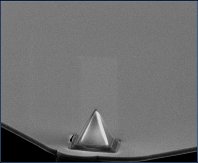 |
| SEM image of a silicon microcantilever with an ultrasharp tip of diamond-like carbon with silicon. (Image: Harish Bhaskaran, IBM) |
| Bhaskaran, a researcher in the nanofabrication group at IBM Research in Zurich (and presently at Yale University), is first author of a paper in the January 31, 2010 online issue of Nature Nanotechnology ("Ultralow nanoscale wear through atom-by-atom attrition in silicon-containing diamond-like carbon") that describes batch fabrication of ultrasharp diamond-like carbon tips that contain significant amounts of silicon on standard silicon microcantilevers for use in atomic force microscopy. |
| "So far, no one has been able to show that materials that 1) one can make controlled nanoscale structures using diamond-like materials and 2) exhibit good tribological characteristics at macroscopic scales are necessarily wear resistant at the nanoscale," Bhaskaran tells Nanowerk. "The latter was mostly because it has been difficult to both fabricate nanoscale structures, as well as test them carefully. Furthermore, work on wear at the nanoscale is rarely quantified – most conclusions are based on qualitative discussions." |
| In this recent work, the IBM-led team, along with Robert Carpick's group at University of Pennsylvania and Kumar Sridharan?s group at University of Wisconsin, not only show they can use a novel material and make true nanoscale structures, but they also quantify the results of this wear resistance – 1 atom per micrometer of sliding when normalized to 1nN of normal force. This knowledge of wear resistance is an important prerequisite for futuristic nanomechanical devices. |
| In fact, IBM researchers will continue to explore this science even further in the new Nanoscience lab that is currently underdevelopment at their Ruschlikon location. The $90 million lab, which will open in the Spring 2011, is a joint effort with ETH Zurich to collaboratively and other partners to further explore this science as well as spintronics, optical interconnects and photonics, just to name a few. This work is an example of how IBM's collaborative efforts have helped drive innovation. |
| The team team of IBM researchers, along with Carpick and Sridharan's groups, found that their novel tips drastically reduce wear at the nanoscale – they were able to demonstrate a wear rate of one atom per micrometer of sliding on silicon dioxide – thus enabling probe based data storage devices to become more reliable. This is especially important for archival storage applications. The long term applications are limited only by what nanomechanical engineers achieve in future. |
| Bhaskaran says that, potentially, this work could revolutionize the commercialization of probe-based lithography, nanometrology and nanomanufacturing. |
| "Given that Si-DLC is also chemically quite inert, it could have wide impact in the bioengineering field, where this property of nanoscale tips is very important. In addition, Si-DLC shows low wear in humid conditions – something that is extremely difficult to achieve at the nanoscale; and important or emerging bio-nano applications – especially using silicon or silicon nitride, as those tips tend to wear very quickly because of tribochemical etching." He adds "Of course, I think we are at the beginning and we still have a long way to go before we can claim to understand everything about nanoscale wear." |
 By
Michael
Berger
– Michael is author of four books by the Royal Society of Chemistry:
Nano-Society: Pushing the Boundaries of Technology (2009),
Nanotechnology: The Future is Tiny (2016),
Nanoengineering: The Skills and Tools Making Technology Invisible (2019), and
Waste not! How Nanotechnologies Can Increase Efficiencies Throughout Society (2025)
Copyright ©
Nanowerk LLC
By
Michael
Berger
– Michael is author of four books by the Royal Society of Chemistry:
Nano-Society: Pushing the Boundaries of Technology (2009),
Nanotechnology: The Future is Tiny (2016),
Nanoengineering: The Skills and Tools Making Technology Invisible (2019), and
Waste not! How Nanotechnologies Can Increase Efficiencies Throughout Society (2025)
Copyright ©
Nanowerk LLC
|

Become a Spotlight guest author! Join our large and growing group of guest contributors. Have you just published a scientific paper or have other exciting developments to share with the nanotechnology community? Here is how to publish on nanowerk.com. |
