| Posted: Mar 05, 2007 |
Novel carbon nanomaterial combines benefits of fullerenes and nanotubes |
| (Nanowerk Spotlight) Carbon comes in many different forms, from the graphite found in pencils to the world's most expensive diamonds. While diamonds might be very popular among ladies, the two most celebrated carbon materials among nanotechnology scientists are fullerenes and carbon nanotubes. What makes them so interesting are the many advantageous properties that they exhibit. Despite the similarities between these two forms of carbon, there have been very few attempts to physically merge them. |
| An international research group, led by a Finnish team, now has discovered a novel hybrid material that combines fullerenes and single-walled carbon nanotubes (SWCNTs) into a single structure in which the fullerenes are covalently bonded to the outer surface of the SWCNTs. In this newly discovered material, that the researchers termed NanoBuds, the fullerene molecules are attached to the outside surface of the carbon nanotubes, just like buds on the branch of a tree - hence the name - and can be made in a simple one-step process. |
| These NanoBuds have been shown to be extremely efficient electron emitters and have excellent electrical conductive properties. In fact, as NanoBuds combine the chemical reactivity of fullerenes and electrical, optical as well as mechanical properties of carbon nanotubes, they may one day replace current materials in many products. Research is continuing to explore NanoBuds’ properties with a view to using them in a wide range of applications. |
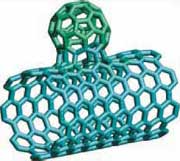 |
| One of the bonding scenarios for a fullerene - SWCNT hybrid structure, reminiscent of buds on a branch. (Reprinted with permission from Nature Publishing Group) |
| "We selectively synthesized the NanoBuds in two different one-step continuous methods, during which fullerenes were formed on iron-catalyst particles together with SWCNTs during CO disproportionation" Dr. David Brown explains to Nanowerk. "The field-emission characteristics of NanoBuds suggest that they may possess advantageous properties compared with SWCNTs or fullerenes alone, or in their nonbonded configurations." |
| Brown, a senior research scientists in Professor Esko I. Kauppinen's NanoMaterials Group at Helsinki University of Technology in Finland, is co-author of a recent paper in Nature Nanotechnology ("A novel hybrid carbon material") that describes the new material. |
 |
| STM topographic image of a fullerene on the surface of a SWCNT. The fullerene appears as a bright area on the SWCNT. The size of the imaged area is 3.29 x 6.57 nm. (Reprinted with permission from Nature Publishing Group) |
| "One of the applications for NanoBuds is as electron sources for new kinds of so called field emission displays (FED) and backlights since the low energy needed to emit electrons means low energy field emmision lights and displays would also be possible" says Brown. "Other researcher have attempted to use carbon nanotubes for this purpose in the past, but, since nanotubes only emit from the tips, they must be aligned to field emit efficiently. NanoBuds solve this problem since they can be deposited randomly and still have excellent field emission properties." |
| NanoBuds also have applications in transparent and conductive flexible thin films for use in, for instance, next generation flexible displays, electronics and solar cells. Other properties suggest uses in super strong concrete and even gene therapy. |
| The researchers synthesized NanoBuds in two different continuous aerosol (floating catalyst) reactors, by using particles grown in situ via ferrocene vapor decomposition and by using premade iron-catalyst particles produced by a hot wire generator. Transmission electron microscope (TEM) images of the product at low magnifications suggest that most synthesized SWCNTs have an ‘amorphous coating’. However, careful investigations revealed that much of the coating in fact consists of fullerenes. |
| "We were also able to control the degree of SWCNT coverage with fullerenes – that is, the degree of SWCNT functionalization – by varying the reactor temperature and the concentrations of water vapor and carbon dioxide" says Brown. "We found that these parameters noticeably affect the amount of fullerenes on the surface of the SWCNTs." |
| The researchers point out that their synthesis method is continuous, does not require multiple processing steps, and allows direct, ambient temperature deposition on any substrate, thereby eliminating the need for supporting substrates to tolerate NanoBud growth temperatures. |
| "The major challenge going forward is how to integrate this material into more complex components, such as electronic circuitry" says Brown. |
| Nevertheless, in order to realize the huge market potential of this novel carbon nanomaterial, some of the researchers (Esko Kauppinen, David Brown, Albert Nasibulin and Hua Jiang) co-founded a company called Canatu Ltd., a spin-off of the Helsinki University of Technology. The company has patent applications on the novel material and all elements of the synthesis, characterization and component manufacturing processes. |
| One of the applications Canatu will actively develop is as NanoBud electron sources for new kinds of so called “field emission” backlights and displays (FED) since the low energy needed to emit electrons means low energy FED lights and displays would also be possible. |
 By
Michael
Berger
– Michael is author of four books by the Royal Society of Chemistry:
Nano-Society: Pushing the Boundaries of Technology (2009),
Nanotechnology: The Future is Tiny (2016),
Nanoengineering: The Skills and Tools Making Technology Invisible (2019), and
Waste not! How Nanotechnologies Can Increase Efficiencies Throughout Society (2025)
Copyright ©
Nanowerk LLC
By
Michael
Berger
– Michael is author of four books by the Royal Society of Chemistry:
Nano-Society: Pushing the Boundaries of Technology (2009),
Nanotechnology: The Future is Tiny (2016),
Nanoengineering: The Skills and Tools Making Technology Invisible (2019), and
Waste not! How Nanotechnologies Can Increase Efficiencies Throughout Society (2025)
Copyright ©
Nanowerk LLC
|

Become a Spotlight guest author! Join our large and growing group of guest contributors. Have you just published a scientific paper or have other exciting developments to share with the nanotechnology community? Here is how to publish on nanowerk.com.
