| Posted: Jul 30, 2010 |
Novel electrical confinement method fabricates uniform quantum dots based on quantum well |
| (Nanowerk Spotlight) Quantum dots have been receiving extensive attention from researchers because they can be widely used for basic physics study, quantum computing, biological imaging, nanoelectronics, and photonics applications. |
| Current major fabrication methods for semiconductor quantum dots include self-assembled growth (Stranski–Krastanov growth), electron beam lithography pattering of top gates on semiconductor heterostructures, and wet/dry etching of semiconductor layers. The Stranski-Krastanov growth method has been widely used for producing highly efficient photonic devices, such as quantum dot infrared photodetectors and photovoltaic devices. However, researchers are struggling with the various drawbacks of these fabrication techniques. |
| The major issues for the self-assembled growth method are the nonuniformity of the quantum dots and the lack of control over positioning of individual quantum dots. The nonuniformity can greatly degrade the performance of quantum dot devices because different sizes of quantum dots have different absorption and emission spectra. |
| As far as e-beam patterning of top metallic gates on semiconductor heterostructure is concerned, this method uses the electrical potential to deplete the electron/hole gas in the heterostructure and form three-dimensional confinement for electrons/holes (forming a quantum dot). These quantum dots are mainly of interest for experiments and applications involving electron or hole transport such as single electron transistor. Furthermore, e-beam lithography is a slow and expensive process. |
| Finally the wet/dry etching of semiconductor – this process uses nanolithography methods to transfer nanopatterns to semiconductors by dry/wet etching. This method creates a lot of surface states and defects on the semiconductor surface, which could severely limit the performance of the quantum dots. |
| "Comparing all these methods, the electrical depletion method has many advantages, such as electrical tunability by gate contacts, smooth confinement boundaries, good control and uniformity if the top gate patterns are uniform enough," Wei Wu explains to Nanowerk. "In our recent work we have, for the first time, applied the electrical depletion method to quantum wells and generate a large area of uniform quantum dots using a uniform metallic nanoholes array on top of quantum wells. This design for forming quantum dots has inherited all the advantages of the electrical depletion method. Furthermore, it can produce millions of uniform quantum dots easily, precisely, and controllably, which will help realize the wide applications of quantum dots in many areas. The uniform nanoholes array can be produced by a high-throughput and low-cost nano-processing technique, superlens lithography technique, developed by the same group." |
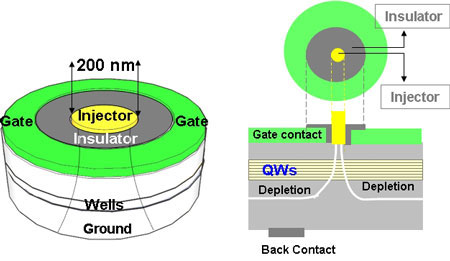 |
| Left: Schematic picture of the quantum dot photodetector device structure. Right: Schematic diagram of an electrically tunable quantum dot device. (Reprinted with permission from American Institute of Physics) |
| Wu, a PhD candidate in Hooman Mohseni's Bio-inspired Sensors and Optoelectronics Laboratory at Northwestern University's Electrical Engineering and Computer Science department, is first author of a recent paper in Applied Physics Letters ("Modeling and fabrication of electrically tunable quantum dot intersubband devices") where the team describes their idea of forming quantum dot intersubband transition devices based on lateral electrical confinement on quantum wells. |
| To apply a lateral field on quantum well layers, the team designed a device structure where gate contact, the insulator below the gate, and semiconductor quantum well layers form a metal-insulator-semiconductor structure. |
| "With different gate voltages, different depletion widths in the quantum wells were formed and thus the quantum dot size is effectively changed" explains Wu. |
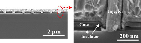 |
| Left: Side view of the nanoholes filled with Ti/Au top injector; and right: the zoomed in view of a single quantum dot. (Reprinted with permission from American Institute of Physics) |
| The above processing technique can be used to fabricate quantum dot infrared photodetectors (QDIP). Researchers have theoretically and experimentally demonstrated superior performances of QDIPs compared with the state of the art quantum well infrared photodetectors (QWIPs). |
| According to Wu, QWIPs currently still require a very low operating temperature due to high thermionic emission rates and n-type QWIP cannot detect normal incidence radiation due to polarization selection rules. "QDIPs can effectively overcome these limitations because of the three-dimensional quantum confinement in the quantum dots" he says. |
| "However, the QDIPs currently produced by the widely used self-assembled growth method still cannot achieve the expected performance and one of the primary suspects for the low performance is quantum dot size nonuniformity. In contrast, the quantum dots produced by our electrical confinement method are very uniform, so we could apply them to infrared detection applications and overcome the problems of the self-assembled quantum dots." |
| In a second paper, in Journal of Physics D: Applied Physics ("A voltage tunable quantum dot photodetector for terahertz detection"), Wu and his colleagues demonstrate a voltage tunable QDIP to detect electromagnetic radiation in the terahertz region. The quantum dots are formed by electrical confinements applied on quantum wells, according to the above technique. |
| "Terahertz frequency range stands between optics and electronics in the electromagnetic spectrum and has potential applications in many areas, such as chemical sensing, medical imaging, and free-space optical communications" says Wu. "However, due to a lack of mature techniques in terahertz emitters and detectors, terahertz technology has still not been fully developed and widely applied yet. We have studied the theoretically work in such a terahertz detector and our simulation results demonstrate a good performance of the detector with an electrical tunability of detection frequency from ∼3.3 THz to ∼12.5 THz." |
| A next step would be to experimentally realize such a low-dimensional electrically tunable intersubband device and to apply this technique in different devices applications such as for instance high performance lasers. |
| "The biggest challenges facing future research are how to successfully fabricate such a complicated and novel three-terminal nanophotonic device" says Wu. "There are more than 50 processing steps to finalize the device and any step failure could lead to device failure." |
 By
Michael
Berger
– Michael is author of four books by the Royal Society of Chemistry:
Nano-Society: Pushing the Boundaries of Technology (2009),
Nanotechnology: The Future is Tiny (2016),
Nanoengineering: The Skills and Tools Making Technology Invisible (2019), and
Waste not! How Nanotechnologies Can Increase Efficiencies Throughout Society (2025)
Copyright ©
Nanowerk LLC
By
Michael
Berger
– Michael is author of four books by the Royal Society of Chemistry:
Nano-Society: Pushing the Boundaries of Technology (2009),
Nanotechnology: The Future is Tiny (2016),
Nanoengineering: The Skills and Tools Making Technology Invisible (2019), and
Waste not! How Nanotechnologies Can Increase Efficiencies Throughout Society (2025)
Copyright ©
Nanowerk LLC
|

Become a Spotlight guest author! Join our large and growing group of guest contributors. Have you just published a scientific paper or have other exciting developments to share with the nanotechnology community? Here is how to publish on nanowerk.com. |
