| Posted: Oct 06, 2010 |
Direct-growth fabrication for paper-based electronics |
| (Nanowerk Spotlight) In the not too distant future, we will be surrounded by miniature and often invisible electronic devices that will be printed on anything you can imagine – paper, fabric, leather, even human tissue (see "Nanotechnology electronics at the tip of your gloved finger"). This in turn enables applications like smart cards on paper; intelligent sensors and electronics on doctors' surgical gloves; health monitors printed on T-shirts; diagnostic devices embedded in your baby's diapers; human-machine interfaces on workers' leather gloves; pollution-monitoring wallpaper; electronic contact lenses; interactive food labeling. You get the idea. |
| One area where researchers are developing innovative techniques is the use of paper or paper-like substrates for printed basic electronics components. Electronic paper displays are already a commercial reality and prototypes of things like paper batteries are under development (see "Nanotechnology sparks energy storage on paper and cloth"). In these applications, researchers transfer thin-films, nanoparticles or other nanostructures onto the desired substrate via various processes. |
| Various methods like chemical, thermal, spin coating, spray pyrolysis, pulsed laser deposition have been used for thin-film formation but they are limited to solid supports such as metal, metal oxides, glass or other thermally stable substrates. By being able to grow these nanostructures directly onto the substrates, scientists hope to get rid of the often energy-consuming and expensive transfer processes. This has already been demonstrated on a large scale on metal substrates ("Growing semiconducting nanostructures directly on conducting metal substrates"). |
| Researchers in Taiwan have now shown, for the first time, that they can directly grow vertically aligned, highly crystalline and defect-free single-crystalline zinc oxide nanorods and nanoneedles on paper as well. |
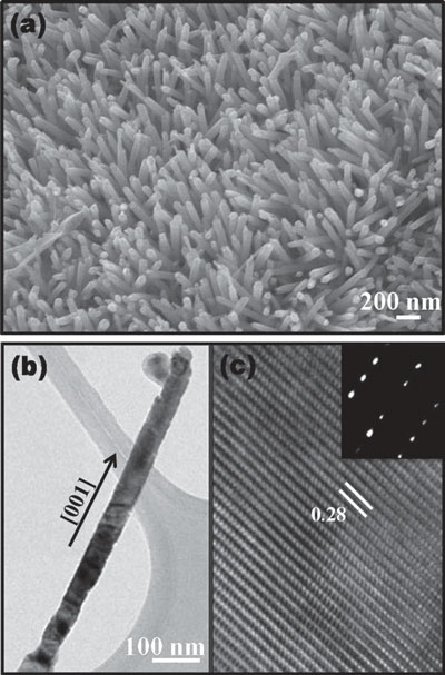 |
| a) Representative FESEM image of aligned ZnO nanorods. b) TEM image of a single nanorod. c) HRTEM image taken from the edge of the ZnO nanorod. Inset: Corresponding SAED pattern. (Reprinted with permission from Wiley-VCH Verlag) |
| Zinc oxide (ZnO) is considered a workhorse of technological development exhibiting excellent electrical, optical, and chemical properties with a broad range of applications as semiconductors, in optical devices, piezoelectric devices, surface acoustic wave devices, sensors, transparent electrodes, solar cells, antibacterial activity etc. Thin films or nanoscale coating of ZnO nanoparticles are viewed with great interest for their many potential applications as substrates for functional coatings. |
| Reporting their findings in a recent issue of Advanced Materials ("Direct Growth of Aligned Zinc Oxide Nanorods on Paper Substrates for Low-Cost Flexible Electronics"), researchers from the Department of Materials Science and Engineering at National Tsing Hua University have fabricated prototype hybrid junction diodes and UV photodetectors based on ZnO nanorod arrays on paper. |
| Initially, the team synthesized aligned ZnO nanowires on a piece of paper that predominantly contains cellulose and calcium carbonate (conventionally paper is synthesized from cotton/pulp and its major components are cellulose, calcium carbonate, silicates, and binders). |
| "The intrinsically rough nature of paper's surface, its insulating properties, damage, and instability during the synthesis process are sizeable inconveniences in realizing potential nanoelectronic devices on paper substrates" explains Lih-Juann Chen, who led the research. "In order to overcome these difficulties we have shown that the paper surface can be modified to different platforms such as conducting and semiconducting surfaces and can be protected from the external environment by being coated with a protective polymer layer." |
| These surface modifications not only provide a conducting platform but also reduce surface roughness and damage occurring during synthesis, and they greatly enhance the alignment and uniformity of ZnO nanowires on the paper substrate. |
| In order to demonstrate the potential for organic/inorganic hybrid junction devices on paper substrates, the team fabricated p-n junction diodes with an average active junction of 1 cm ? 1 cm using zinc oxide nanowires with 90 nm diameter and 1.5 µm length, grown on a 50 nm gold-coated paper substrate. |
| The researchers point out that stable electrical performance of hybrid devices at different bending or twisting positions is a critical challenge for flexible substrates. For this reason, they measured the electrical/mechanical fatigue properties of the diode at different bending positions across the junction area. |
| They found that there is only negligible difference in the turn-on voltage of the devices while the forward current at high voltage is slightly decreased with increase of bending angle. Repetitive bending of the diode affected the performance only marginally. |
| "We anticipate versatile applications for these zinc oxide nanostructures on paper in flexible, portable electronic gadgets and display devices as well as in biomedical applications – these are under investigation" says Chen. "We foresee a productive future for the direct growth of one-dimensional nanostructures on paper substrates, paving the way to low-cost, high-performance devices beyond the range of conventional technology. Innovative concepts and strategies are required to engineer materials and devices on such an exceptionally flexible platform." |
 By
Michael
Berger
– Michael is author of four books by the Royal Society of Chemistry:
Nano-Society: Pushing the Boundaries of Technology (2009),
Nanotechnology: The Future is Tiny (2016),
Nanoengineering: The Skills and Tools Making Technology Invisible (2019), and
Waste not! How Nanotechnologies Can Increase Efficiencies Throughout Society (2025)
Copyright ©
Nanowerk LLC
By
Michael
Berger
– Michael is author of four books by the Royal Society of Chemistry:
Nano-Society: Pushing the Boundaries of Technology (2009),
Nanotechnology: The Future is Tiny (2016),
Nanoengineering: The Skills and Tools Making Technology Invisible (2019), and
Waste not! How Nanotechnologies Can Increase Efficiencies Throughout Society (2025)
Copyright ©
Nanowerk LLC
|

Become a Spotlight guest author! Join our large and growing group of guest contributors. Have you just published a scientific paper or have other exciting developments to share with the nanotechnology community? Here is how to publish on nanowerk.com. |
