| Posted: Oct 14, 2010 |
Electrofluidics device uses sub-10nm nanochannels to analyze DNA |
| (Nanowerk Spotlight) In order to improve throughput speed of DNA sequencing and reduce its cost, researchers are pursuing real-time solid-state DNA sequencing devices. To that end, electronic functional devices in liquid environments need to be developed, ideally utilizing the compatibility with current complementary metal oxide semiconductor (CMOS) based fabrication technology. In this regard, the combination of electronics and nanofluidics leads to the field of electrofluidics, which utilizes the electrical behaviors of fluids for solid state device applications. |
| "Electrical rectifying or gating functions have been demonstrated in electrofluidic devices; nanopores and nanochannels have shown diode or transistor components" Ki-Bum Kim, who leads the Nano Fabrication Laboratory at Seoul National University in Korea, explains to Nanowerk. "These devices serve as good platforms to study biomolecular motion, such as DNA translocation or DNA recoiling, in which the underlying sensing or detecting mechanisms have been studied. However, the active manipulations of biomolecules in an electrical manner, such as trapping, capturing, and controlling the speed of the motion, are still ongoing subjects which have significant implications for the ultimate goal of solid state DNA sequencing device." |
| To sequence a DNA molecule – which is negatively charged and is only a few nanometers wide – it is important to control the transport of DNA in a confined structure. This confined structure should be less than 10 nm in diameter. |
| In electrofluidics, the control of surface charge in fluidic channels is a key issue – the ion concentration inside the channel will strongly affect the transport of the DNA molecule. In previous work dealing with electrofluidic applications, Kim's team has designed nanopores to have an embedded electrode that serves to manipulate KCl electrolyte ions ("Ionic Field Effect Transistors with Sub-10 nm Multiple Nanopores"). This concept, namely ionic field effect transistor (IFET), is similar to the semiconductor field effect transistor (FET) except that the channel medium is made of electrolyte ions instead of electrons or holes. |
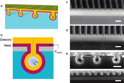 |
| The concept of all around gating (AAG) ionic field effect transistor (IFET) (gray, amorphous silicon; cyan, SiO2; yellow, ALD dielectric film; purple, ALD metal film). (a) Schematic picture of nanochannel AAG-IFET. (b) The ionic strength within the nanochannel can be controlled by electric gate bias (VGATE), when the channel size becomes as small as Debye screening length (λD). Cross-sectional SEM images of (c) trench, (d) pipe, and (e) core/shell nanochannels. Nanochannels are surrounded by Al2O3 dielectric/Ru metal. Scale bars are (c, d) 250 nm, (e) 100 nm (top), and 250 nm (bottom). (reprinted with permission from American Chemical Society) |
| In order to explore the ion transport and biomolecule transport through nanochannels, Kim's team has now reported ("Sub-10-nm Nanochannels by Self-Sealing and Self-Limiting Atomic Layer Deposition") the fabrication of an electrofluidic platform to study the motion of single molecules, including DNA. The device's nanochannel structures were fabricated with sub-lithographic dimension through top-down based, conventional semiconductor fabrication methods. |
| In contrast to the previous work, where the vertical type of device using a nanopore structure has been difficult to integrate as a chip, the new work presents similar results but is made by using nanochannels. Such a nanochannel structure is much easier to be integrated as a chip. |
| "Our main claim in this paper was the demonstration of ion-field effect transistor in 'sub-10 nm' nanochannel structures" says Kim. "The fabrication process includes e-beam lithography and atomic layer deposition (ALD) which is commonly used in conventional semiconductor processing. Thus, the structure is much more robust compared to other processes suggested so far. Moreover, this structure has all-around metal gate surrounding the nanochannels which makes it possible to control both the types and the concentration of ions inside of the channel." |
| The researchers point out that the ALD process has two unique advantages for the nanochannel fabrication. "First, the conformal film deposition can allow for a self-sealing process of nanochannels during the ALD, if the film thickness is adequate to cover the whole trench region. Second, the diameter of the nanochannel is automatically determined during the ALD regardless of the deposited ALD film thickness." |
| Kim believes that the nanochannel structures with sub-10nm dimension promise to be an interesting electrofluidic platform to study the motion of single molecules, including DNA. "This reliable nanochannel fabrication method at dimensions well below the lithographic limit may provide a novel means for nanofluidic or electrofluidic applications." |
| The team is now working on fine-tuning their control of the DNA transport through the nanochannels. But DNA is just one examples. Basically, any biomolecule which has a certain charge can be controlled with this device. |
 By
Michael
Berger
– Michael is author of four books by the Royal Society of Chemistry:
Nano-Society: Pushing the Boundaries of Technology (2009),
Nanotechnology: The Future is Tiny (2016),
Nanoengineering: The Skills and Tools Making Technology Invisible (2019), and
Waste not! How Nanotechnologies Can Increase Efficiencies Throughout Society (2025)
Copyright ©
Nanowerk LLC
By
Michael
Berger
– Michael is author of four books by the Royal Society of Chemistry:
Nano-Society: Pushing the Boundaries of Technology (2009),
Nanotechnology: The Future is Tiny (2016),
Nanoengineering: The Skills and Tools Making Technology Invisible (2019), and
Waste not! How Nanotechnologies Can Increase Efficiencies Throughout Society (2025)
Copyright ©
Nanowerk LLC
|

Become a Spotlight guest author! Join our large and growing group of guest contributors. Have you just published a scientific paper or have other exciting developments to share with the nanotechnology community? Here is how to publish on nanowerk.com. |
