| Posted: May 16, 2007 |
Carbon nanotubes to the rescue of Moore's law |
| (Nanowerk Spotlight) Over the next few years, semiconductor fabrication will move from the current state-of-the-art generation of 90 nanometer processes to the next 65 nm and 45 nm generations. Intel is even already working on 32 nm processor technology, code-named "Westmere", that is expected to hit the market sometime around 2009. The result of these efforts will be billion-transistor processors where a billion or more transistor-based circuits are integrated into a single chip. One of the increasingly difficult problems that chip designers are facing is that the high density of components packed on a chip makes interconnections increasingly difficult. |
| In order to be able to continue the trend predicted by Moore’s law, at least for a few more years, researchers are now turning to alternative materials for transistors and interconnect and one of the prime candidates for this job are single-walled carbon nanotubes (SWCNT). However, one of the biggest limitations of conventional carbon nanotube device fabrication techniques today is the inability to scale up the processes to fabricate a large number of devices on a single chip. |
| Researchers in Germany have now demonstrated the directed and precise assembly of single-nanotube devices with an integration density of several million devices per square centimeter, using a novel aspect of nanotube dielectrophoresis. This development is a big step towards commercial realization of CNT-based electronic devices and their integration into the existing silicon-based processor technologies. |
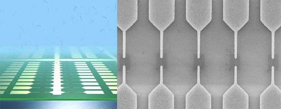 |
| The image on the left shows a schematic of an ultra-large scale array of single-walled carbon nanotube devices fabricated by dielectrophoretic deposition from an aqueous solution. The scanning electron micrograph on the right shows the zoom-in to one region of the array showing each electrode pair bridged by an individual carbon nanotube in a self-limiting mechanism. (Images: Dr. Vijayaraghavan, Dr. Krupke, Forschungszentrum Karlsruhe) |
| "The fundamental issue of CNT device fabrication remains the biggest challenge for effective commercialization of nanotube electronics" Dr. Ralph Krupke explains to Nanowerk. "For CNT electronics to become a reality, it should be possible to scale up the fabrication technique to simultaneously and reproducibly fabricate a very large number of such devices on a single chip, each accessible individually for electronic transport. Conventional nanotube growth and device fabrication techniques using chemical vapor deposition or spin-casting are unable to achieve this, due to a lack of precise control over nanotube positioning and orientation." |
| "Since these nanotubes are usually grown at temperatures greater then 500°C and show no growth selectivity between metallic and semi-conducting types, they can not be directly integrated into silicon-based micro-fabrication" adds Dr. Aravind Vijayaraghavan. "Due to the difficulties in handling and manipulating these nano-scale objects at the individual level, various attempts to assemble them into functional devices have met with limited success. In the ideal case, it should be possible to position an individual nanotube at a predefined location and orientation, forming robust, low-resistance, ohmic contacts to two metallic leads. Furthermore, it should be possible to do this at a scalable integration density with each nanotube forming an individually addressable device." |
| Krupke and Vijayaraghavan are scientists at the Institute of Nanotechnology (INT) at the Research Center Karlsruhe in Germany. Together with colleagues from the INT and the University of Karlsruhe they authored a recent paper in Nano Letters, titled "Ultra-Large-Scale Directed Assembly of Single-Walled Carbon Nanotube Devices". In it, they report a novel aspect of dielectrophoretic deposition of CNTs, where the dielectrophoretic force field changes upon nanotube deposition and thereby self limits the directed assembly to a single nanotube or nanotube bundle at predefined locations. |
| In 2003, the group demonstrated that it is possible to deposit CNT bundles from an aqueous solution using a process called dielectrophoresis which uses inhomogeneous alternating electric fields to move and assemble nano-scale objects. |
| "Since then, we have made tremendous advances in understanding the dynamics of a carbon nanotube moving in such an electric field" says Vijayaraghavan. "The required inhomogeneous electric fields are generated by two opposing needle-shaped electrodes with a microscopic gap between their tips. We have discovered the mechanism that allows for a self-limiting deposition of CNTs to one per electrode pair. This happens because the first CNT that is deposited in the gap changes the electric field distribution around it incisively, leading to a repulsion of subsequent CNTs that attempt to enter the region of the gap." |
| The researchers in Karlsruhe have also developed and optimized the use of capacitively coupled electrodes, which enables them to reduce their dimensions and increase the density of electrode pairs that can be incorporated on a chip. |
| "Together, this allows us to fabricate separately addressable, individual SWCNT devices at an integration density comparable to ultra-large scale integration" says Krupke. "This is three to four orders of magnitude greater than what has been possible so far with any other technique." |
| This technique is very versatile. It is compatible with SWCNTs from any source, which are suitably dispersed in an aqueous surfactant solution. SWCNTs separated based on their length, diameter or even chirality can be readily assembled into large-scale functional arrays using this technique. The process is fully compatible with post-processing techniques and current microelectronics fabrication technologies, requires no high-temperature steps or chemical modification of the substrate or the CNT and is a one-step process that can be performed under ambient conditions. |
| This achievement takes CNT electronic devices a big step closer to integrating with microelectronics and expanding their scope for commercial viability. On a laboratory scale, it now allows for the fabrication of a large number of devices with identical CNT source and deposition conditions, to perform truly statistical measurements of CNT properties like electronic transport or Raman mapping. |
 By
Michael
Berger
– Michael is author of four books by the Royal Society of Chemistry:
Nano-Society: Pushing the Boundaries of Technology (2009),
Nanotechnology: The Future is Tiny (2016),
Nanoengineering: The Skills and Tools Making Technology Invisible (2019), and
Waste not! How Nanotechnologies Can Increase Efficiencies Throughout Society (2025)
Copyright ©
Nanowerk LLC
By
Michael
Berger
– Michael is author of four books by the Royal Society of Chemistry:
Nano-Society: Pushing the Boundaries of Technology (2009),
Nanotechnology: The Future is Tiny (2016),
Nanoengineering: The Skills and Tools Making Technology Invisible (2019), and
Waste not! How Nanotechnologies Can Increase Efficiencies Throughout Society (2025)
Copyright ©
Nanowerk LLC
|

Become a Spotlight guest author! Join our large and growing group of guest contributors. Have you just published a scientific paper or have other exciting developments to share with the nanotechnology community? Here is how to publish on nanowerk.com.
