| Posted: Dec 13, 2010 |
Novel, fast DNA nanopore detector features integrated tunneling electrodes |
| (Nanowerk Spotlight) Researchers worldwide are working on fast and low-cost strategies to sequence DNA, that is, to read off the content of our genome. Particularly promising for future genome sequencing are devices that measure single molecules. Imagine a single DNA molecule from one of your cells – 3 billion bases, 1 meter long if you would stretch it from head to tail – that is read, base per base, in real time while sliding between two of your fingers. |
| In this respect, the creation of nanochannels or nanopores in thin membranes has attracted much interest due to the potential to isolate and sense single DNA molecules while they translocate through the highly confined channels (see for instance: "Sucking nanospaghetti through nanopores - the art of single-molecule spectroscopy"). |
| Particularly interesting are techniques that can offer fast and low cost readout of long DNA molecules without the need of DNA labelling or amplification. In very interesting work performed at Imperial College London, researchers have now successfully developed a protocol for the fabrication of a solid state nanopore aligned to a tunneling junction. |
| In a paper in the December 6, 2010 online edition of Nano Letters ("DNA Tunneling Detector Embedded in a Nanopore"), they present a simple but powerful approach to fabricate tunneling junctions aligned to a nanopore and perform proof-of-principle experiments demonstrating simultaneous detection of DNA translocations using both tunneling and ionic currents in a nanopore platform. |
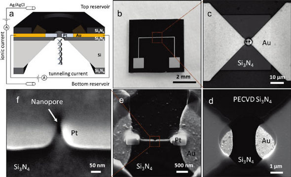 |
| (a) Schematic of the nanopore/nanogap device integrated into an electrochemical cell. The tunneling junction is located at the exit of the nanopore. DNA is inserted in the bottom reservoir and electrophoretically driven through the nanopore and the tunneling junction. (b) Optical image of the 5 mm x 5 mm chip. (c) Free-standing 40 µm x 40 µm Si3N4 membrane aligned to the gold microelectrodes. (d) SEM image of the window in the PECVD Si3N4 layer opened by RIE. (e) SEM image of the platinum nanoelectrodes fabricated by EBID. The additional platinum contact pads (250 x 500 nm) were deposited to improve electrical connection to the gold microelectrodes. (f) Magnified SEM image showing the nanopore aligned to the platinum nanoelectrodes. (Reprinted with permission from American Chemical Society) |
| "Our work combines two recent and very powerful techniques for the real time label free detection and analysis of single biological molecules in solution," Aleksandar P. Ivanov explains to Nanowerk. "One is nanopore detection with ionic current blockade, where a nanoscale aperture – a nanopore – is used to connect two electrolyte filled compartments. Biological molecules such as DNA are pulled through the nanopore by external electric field and briefly block the ionic current through the pore, which allow us to quickly extract molecular properties such as size, composition, even interactions with other biomolecules. This technique is well developed but has some limitations such as spatial resolution and is still debated whether it can be used for DNA sequencing. The other detection technique is based on electron tunnelling phenomena, which can allow higher spatial resolution and has a great potential as a next generation DNA sequencing technology, but currently lacks many of the advantages of nanopore technology, such as detection speed." |
| Ivanov, a student in Joshua Edel's and Tim Albrecht's research groups at Imperial College, and co-first author of the paper together with Emanuele Instuli, points out that it is very challenging to combine the nanopore and the tunnelling junction in a single platform. In effect, what the team has been trying to build is a scanning tunnelling microscope on a nanopore. However, instead of scanning an immobilized DNA molecule with the tip of a tunnelling microscope, they are detecting the molecule by pulling it with an electric field though a tunnelling junction. |
| "There are several studies pioneering this field, however in all these cases the electrode gaps either were large or were not used for the detection of analyte" says Edel. "In our experiments, we were able to fabricate electrode junctions with gap sizes sufficiently small to allow for tunneling transport to occur and precisely align the electrode junction to a nanopore for use in DNA. Furthermore, in proof-of-principle experiments demonstrating, for the first time, concurrent tunneling detection and ionic current detection of DNA molecules in a nanopore platform." |
| Fabrication of the nanopores (50-80 nm diameter) and the electrode junctions was performed using a dual beam focused ion beam (FIB)/ scanning electron microscope (SEM) instrument. This allowed for the entire fabrication and alignment process to be controlled in situ and monitored in real time. Once the pores were milled, the platinum nanoelectrodes were fabricated by electron beam induced deposition (EBID). |
| "Finally, for the fabrication of the tunneling junctions, lateral broadening of the metal deposit has to be taken into account, which decreases the actual gap size compared to the nominal size as defined in the design template" notes Ivanov. "In our experiments, electrode junctions deposited with a nominal gap size of 50-60 nm exhibited tunneling behavior. We further optimized the geometry of the nanogap by performing the deposition at an angle of 54? with respect to the electron beam. This allowed us to exploit the lateral broadening effect to decrease the nanowire width and height in the vicinity of the nanogap" (see figure 1f above). |
| The team performed proof-of-principle experiments using λ-DNA as a test sample and they were successful in detecting DNA translocation events simultaneously in both the ionic and tunneling currents. |
| Ivanov explains that two types of translocation events were recorded: first, type I events occurred on a submillisecond time scale and were recorded only in the ionic current channel. These events were not detected in the tunneling current. Second, type II events consisted of translocations greater than 1ms in duration and were recorded in both the ionic current and tunneling current channels. |
| "The longer translocation time when compared to type I is likely due to either adsorption or trapping in the tunneling junction" he says. |
| Future work in Edel's group will include molecular fragment sizing based on tunnelling and of course DNA sequence specific applications. This work however, is not only limited to DNA, but also has applications in the detection of other fundamentally important biological molecules such as RNA , peptides and proteins. |
| Reference: Ivanov, A., Instuli, E., McGilvery, C., Baldwin, G., McComb, D., Albrecht, T., & Edel, J. (2010). DNA Tunneling Detector Embedded in a Nanopore Nano Letters DOI: 10.1021/nl103873a |
 By
Michael
Berger
– Michael is author of four books by the Royal Society of Chemistry:
Nano-Society: Pushing the Boundaries of Technology (2009),
Nanotechnology: The Future is Tiny (2016),
Nanoengineering: The Skills and Tools Making Technology Invisible (2019), and
Waste not! How Nanotechnologies Can Increase Efficiencies Throughout Society (2025)
Copyright ©
Nanowerk LLC
By
Michael
Berger
– Michael is author of four books by the Royal Society of Chemistry:
Nano-Society: Pushing the Boundaries of Technology (2009),
Nanotechnology: The Future is Tiny (2016),
Nanoengineering: The Skills and Tools Making Technology Invisible (2019), and
Waste not! How Nanotechnologies Can Increase Efficiencies Throughout Society (2025)
Copyright ©
Nanowerk LLC
|

Become a Spotlight guest author! Join our large and growing group of guest contributors. Have you just published a scientific paper or have other exciting developments to share with the nanotechnology community? Here is how to publish on nanowerk.com. |
