| Posted: Jan 05, 2011 |
Nanofabrication enables mass production of non-reflective polymer surfaces |
| (Nanowerk Spotlight) A key hurdle in realizing high-efficiency, cost-effective solar energy technology is the low efficiency of current power cells. In order to achieve maximum efficiency when converting solar power into electricity, ideally you need a solar panel that can absorb nearly every single photon of light – across the entire spectrum of sunlight and regardless of the sun's position in the sky. |
| One way to achieve suppression of sunlight's reflection over a broad spectral range is by using nanotextured surfaces that form a graded transition of the refractive index from air to the substrate. Researchers in Finland have now demonstrated a scalable, high-throughput fabrication method for such non-reflecting nanostructured surfaces. |
| The main advances of this work, published in a recent paper in Advanced Materials ("Non-Reflecting Silicon and Polymer Surfaces by Plasma Etching and Replication"), are in the field of nanofabrication. |
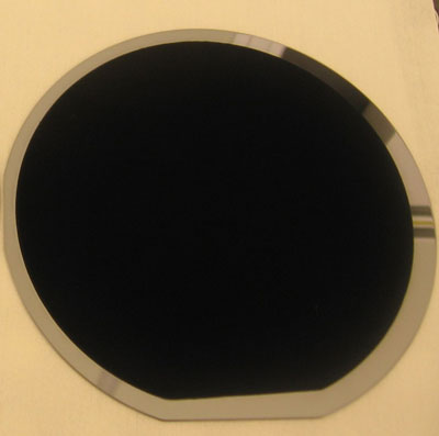 |
| Figure 1: Photograph of nanostructured non-reflective silicon surface. (Image: Lauri Sainiemi, Aalto University School of Science and Technology) |
| "We studied a maskless deep reactive ion etching process that produces nanospikes on a silicon wafer," Lauri Sainiemi tells Nanowerk. "The process is known as black silicon process. We found out that by changing the etching parameters we are able to modify the height, width, density and geometry of nanospikes. The main strength of the maskless method is its high throughput." |
| Sainiemi, first author of the paper, is a post-doc researcher in the Microfabrication Group of the Department of Materials Science and Engineering at Aalto University School of Science and Technology. He explains a key difference between his group's work and previously published studies that utilize maskless etching: "We systematically studied the effect of plasma etching parameters on the final nanostructure and found parameters for creating many different types of nanopillars. The sloping angle, height, aspect ratio and spike density could all be tuned by selecting suitable etching conditions. This is extremely important for extending the usefulness and general significance of the method beyond maskless methods which only produce a single type of structure." |
| Different applications require different types of surfaces, and in this study the Finnish team shows that the densest arrays of nanospikes with slightly positively tapered sidewalls had the lowest optical reflectance, while pyramid-shaped nanospikes were ideal for use as templates for polymer replication. |
| Sainiemi notes that they also found out that the implemented nanospikes-structures with positive sidewall slopes can be replicated into polymers. Polymer replication techniques are typically high-throughput and low-cost methods which make them very attractive. Earlier, the possibility to transfer the antireflective structures into polymers has not had the attention that it deserves in the literature. |
| To do this, first, an elastomeric stamp is produced by casting a PDMS layer on top of the nanospike-structured silicon surface (the original nanospikes were fabricated on full silicon wafers using the black silicon process). The PDMS is thermally cured and peeled off. Then, the PDMS stamp can be used to replicate the original nanospike pattern into other polymers, such as PMMA. |
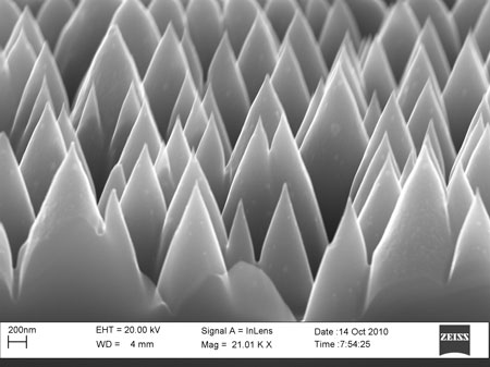 |
| Figure 2: Close-up SEM image of the nanostructured non-reflective silicon surface in figure 1. (Image: Lauri Sainiemi, Aalto University School of Science and Technology) |
| "We demonstrated that both hot-embossing and UV-embossing of polymer is possible with the PDMS stamp" he says. "The use of polymers instead of silicon would be useful in high-volume applications due to lower costs." |
| Nanospike-structured polymeric and silicon surfaces are non-reflective and additionally they can be made ultrahydrophobic and self-cleaning, by coating them with a low-surface energy coating. These kinds of inexpensive, non-reflective and self-cleaning surfaces have many applications, for instance in sensors and solar cells. |
| "Our research group is currently studying similar high throughput fabrication methods for ultrahydrophbic and oleofobic materials that are based on micro- and nanostructured surfaces," says Sainiemi. "It is fairly straightforward to implement ultrahydrophobic surfaces if one can use clean room equipment. Our goal is to develop a straightforward and high throughput fabrication method that can produce versatile nanostructures. Fabrication of nanostructured silicon surfaces requires only one step and the type of nanostructure can be modified by the etching parameters." |
| Another important issue is the mechanical durability of the nanostructured surfaces. At the moment the nanostructured surfaces damage quite easily but the team is studying ways to make the surfaces more robust. |
 By
Michael
Berger
– Michael is author of four books by the Royal Society of Chemistry:
Nano-Society: Pushing the Boundaries of Technology (2009),
Nanotechnology: The Future is Tiny (2016),
Nanoengineering: The Skills and Tools Making Technology Invisible (2019), and
Waste not! How Nanotechnologies Can Increase Efficiencies Throughout Society (2025)
Copyright ©
Nanowerk LLC
By
Michael
Berger
– Michael is author of four books by the Royal Society of Chemistry:
Nano-Society: Pushing the Boundaries of Technology (2009),
Nanotechnology: The Future is Tiny (2016),
Nanoengineering: The Skills and Tools Making Technology Invisible (2019), and
Waste not! How Nanotechnologies Can Increase Efficiencies Throughout Society (2025)
Copyright ©
Nanowerk LLC
|

Become a Spotlight guest author! Join our large and growing group of guest contributors. Have you just published a scientific paper or have other exciting developments to share with the nanotechnology community? Here is how to publish on nanowerk.com. |
