| Posted: Jan 14, 2011 |
Novel nanocharacterization technique for analyzing nanomaterial-substrate bonding |
| (Nanowerk Spotlight) Ranging from electronic gadgets to medical applications, many nanomaterial-based devices have appeared in the market. One of the most important issues for these devices is their reliability and life-time of operation. A vital factor behind these issues is the structural stability of the nano-device – debonding of the nanomaterial from the substrate material being the single largest contribution for device degradation. In order to improve bonding between nanomaterials and their substrate, it is essential to understand and quantify the bonding mechanisms. A new nano-scratch technique developed by researchers in the U.S. could serve as the basis for a reliable quantification technique for interpreting nanomaterial-substrate bond strength. |
| With their new method, a team from Florida International University (FIU) and UC San Diego was able to quantify nanotube-substrate adhesion strength down to an individual nanotube level on different substrates. |
| "Our core idea was to apply a nano-level characterization technique to understand the bonding between a nanomaterial (e.g. carbon nanotube) and its substrate," Wonbong Choi, Associate Professor and Director of Nanomaterials & Device Laboratory, at the Department of Mechanical and Materials Engineering at FIU, tells Nanowerk. "We demonstrated for the first time the debonding energy of nanomaterials with their substrates at a nanoscale-level. Since the bonding is at the nano-level, the nanocharacterization technique has the highest potential to quantify this bonding energy most convincingly." |
| This new technique successfully overcomes limitations of other techniques used so far. Most popular methods are qualitative in nature, like air-blowing, or peeling with a scotch-tape, or ultrasonication etc. Quantitative techniques have also been based on adhesive tape – sticking an adhesive tape onto the material and then applying tensile or shear forces to obtain a strength value at the point of detachment. |
| However, these methods are deficient in several aspects – lack of calibration with respect to standard samples; unknown actual contact area; and unidentified position of breakage (from nanomaterial-substrate interface or from other positions within the nanomaterial or from the tape itself) etc. |
| The new method of nano-scratching developed by Choi and his team overcomes all these limitations and presents a bonding energy value, which can even be calibrated against the effects of substrate, catalyst and interface layer. The bonding energy value, obtained through this method, shows high reliability and reproducibility. The results have been published in the January 5, 2011 online edition of ACS Nano ("Carbon Nanotubes: How Strong Is Their Bond with the Substrate?"). |
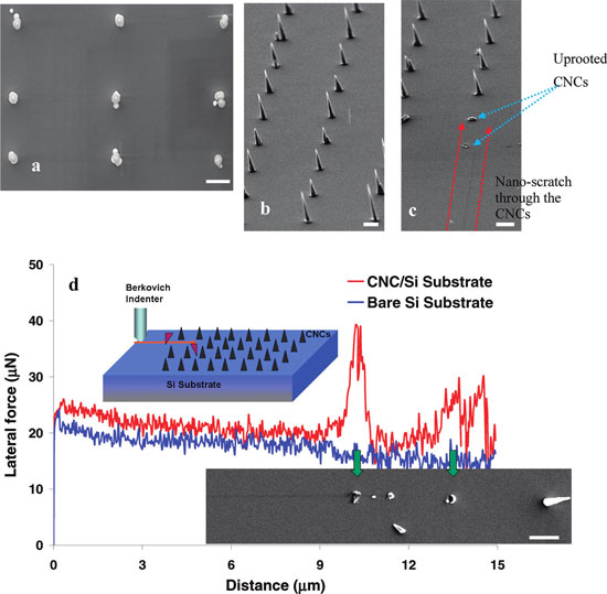 |
| Nanoscratch on nanopatterned carbon nanocone structure. (a-c) SEM images of the carbon nanocone (CNC) structure: (a) before nanoscratch, imaged at a tilt angle of ∼40°; (b) before nanoscratch, imaged from top, showing the presence of multiple CNCs in each catalytic islands; and (c) after nanoscratch showing removal of CNCs, imaged at a tilt angle of ∼40°. (d) Lateral force response during nanoscratch test on the Si-CNC sample, comparing effects on bare substrate and through CNCs. The top inset shows a schematic of the process, uprooted CNCs being shown in a different color. The lower inset shows the corresponding SEM image. All scale bars in this figure are 1 µm. (reprinted with permission from American Chemical Society) |
| "Moreover, we wish to emphasize that previous studies which have addressed the issue of CNT-substrate adhesion, were also performed on a specific CNT growth condition," says Choi. "In all these studies, authors have followed a specific growth condition and then characterized the adhesion strength for that specific sample. Hence, the adhesion values reported by those reports are valid for those specific growth parameters only. In our study also, we have kept the growth conditions 'exactly same' for both Cu and Si substrates and then characterized the bonding between CNT-substrate. The bonding energy values, mentioned in our paper, are true only for the processing conditions used during the present study. We do not claim that CNT-substrate bonding value reported in our study is as a 'universal' value." |
| Choi points out that the development of this methodology was only possible through the collaboration between experts of nanomaterials and devices (Dr. Wonbong Choi and his PhD student Indranil Lahiri), nanomechanics (Dr. Arvind Agarwal at FIU and his PhD student Debrupa Lahiri) and nanoengineering (Dr. Sungho Jin at UCSD). |
| In order to prove the feasibility and applicability of their technique, the team used carbon nanotubes (CNTs) and carbon nanocones for their experiments. The nanoscratch-based technique was applied to quantify bonding energy of CNTs on two different types of substrates, Cu and Si, both having Ti and Ni as barrier layer and catalyst, respectively. |
| Choi notes that, although CNTs can be synthesized on a wide variety of substrates, their choice of Cu substrate is inspired by the team's recent studies, in which randomly oriented multiwall CNT structure, directly grown on Cu substrate, has shown excellent properties for application in Li-ion battery electrodes ("High Capacity and Excellent Stability of Lithium Ion Battery Anode Using Interface-Controlled Binder-Free Multiwall Carbon Nanotubes Grown on Copper") and field emission devices ("Enhanced field emission from multi-walled carbon nanotubes grown on pure copper substrate"), which was attributed to the stable interfacial structure. On the other hand, Si has been the most widely used substrate material for CNT-based devices. |
| The method is a big step forward in understanding and quantifying CNT-substrate bonding energy. Probably the most significant point of this nano-scratch technique is that the process is very simple in operation, independent of operator's skill, highly reproducible and extremely sensitive. |
| Moreover, the method can be applied to any kind of nanomaterial, irrespective of its nature or chemical composition – which means that the technique can be adopted by all researchers and producers of nanomaterial-based components and devices. |
 By
Michael
Berger
– Michael is author of four books by the Royal Society of Chemistry:
Nano-Society: Pushing the Boundaries of Technology (2009),
Nanotechnology: The Future is Tiny (2016),
Nanoengineering: The Skills and Tools Making Technology Invisible (2019), and
Waste not! How Nanotechnologies Can Increase Efficiencies Throughout Society (2025)
Copyright ©
Nanowerk LLC
By
Michael
Berger
– Michael is author of four books by the Royal Society of Chemistry:
Nano-Society: Pushing the Boundaries of Technology (2009),
Nanotechnology: The Future is Tiny (2016),
Nanoengineering: The Skills and Tools Making Technology Invisible (2019), and
Waste not! How Nanotechnologies Can Increase Efficiencies Throughout Society (2025)
Copyright ©
Nanowerk LLC
|

Become a Spotlight guest author! Join our large and growing group of guest contributors. Have you just published a scientific paper or have other exciting developments to share with the nanotechnology community? Here is how to publish on nanowerk.com. |
