| Posted: Feb 22, 2011 |
Nanolasers grown on silicon allow bottom-up nano-optoelectronic integration |
| (Nanowerk Spotlight) Silicon and III-V semiconductors are the respective foundations of modern electronics and photonics. Integrating these materials is essential for achieving new optoelectronic functionality and faster computer architecture. However, lattice mismatch and high III-V growth temperatures have prevented such integration thus far. Most importantly, in order to be able to take advantage of today's massive silicon infrastructure, integration must be compatible with current complementary metal-oxide-semiconductor (CMOS) infrastructure and process flows. |
| Researchers at UC Berkeley have overcome these obstacles by developing a way to grow III-V nanolasers on silicon, demonstrating the potency of bottom-up nano-optoelectronic integration. |
| "The small footprint of our III-V nanopillars allows us to bypass lattice mismatch constraints, and our low growth temperatures mean that our lasers can be integrated in after electronics fabrication in CMOS labs," Connie Chang-Hasnain, John R. Whinnery Chair Professor and Director, Center for Optoelectronic Nanostructured Semiconductor Technologies, tells Nanowerk. "Combined with the natural laser cavity provided by our nanopillars, this has resulted in lasers on silicon, a critical component needed in the future for silicon photonics." |
| Based on previous work ("Core-shell InGaAs/GaAs quantum well nano needles grown on silicon with silicon-transparent emission"), where Chang-Hasnain and her group demonstrated the growth of single-crystal GaAs nano needles on silicon at 400°C under conditions compatible with CMOS technology, the team has now developed InGaAs/GaAs heterostructure nanopillar lasers that are monolithically integrated onto silicon after a single growth step. |
| The results, first-authored by Roger Chen, have been reported in the February 6, 2011 online edition of Nature Photonics ("Nanolasers grown on silicon"). |
| "Other groups have made strides in integrating light sources on silicon by wafer bonding III-V on silicon," explains Chang-Hasnain. "However, this approach faces potential issues with scalability since wafer flatness is required. Another method involves epitaxial thin film, which requires high temperature (>550°C) and can only be integrated at the front-end-of-line (FEOL). This means III-V materials would have to enter dedicated silicon fabrication, inevitably changing CMOS process flows, which would be very costly." |
| By contrast, the Berkeley team has chosen to develop an integration scheme that can be done at back-end-of-line (BEOL). This new approach allows lasers to be integrated after electronics fabrication, thereby leaving electronics process flows undisturbed. |
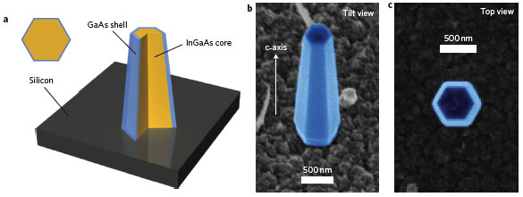 |
| InGaAs/GaAs heterostructure nanopillar lasers monolithically grown on silicon. a, Schematic of a nanopillar laser monolithically integrated onto silicon, illustrating its InGaAs core and GaAs shell. The higher-bandgap GaAs shell protects carriers from non-radiative surface recombination, which is critical for room-temperature lasing. Inset: top-view schematic. b, SEM image showing the well-faceted geometry of the nanopillar optical cavity. This resonator structure forms naturally during growth, allowing lasers to be directly grown on silicon without additional processing. Nanopillar dimensions scale with growth time, enabling the growth of effectively bulk high-quality III–V material on silicon. No critical dimensions have been observed for this novel lattice-mismatched growth mechanism. c, Top-view SEM image highlighting the hexagonal wurtzite crystal structure of the nanopillar. This hexagonal symmetry results in whispering gallery-like effects. (Reprinted with permission from Nature Publishing Group) |
| The nanopillar-based laser fabricated by the team contains InGaAs active region at its core and surface passivation provided by the GaAs shell. These nanopillars have tiny footprints of only ∼0.34 µm2, enabling them to realize high-density silicon-based optoelectronics. |
| "To the best of our knowledge,the as-grown nanopillar structure provides a natural optical cavity supporting unique resonances that have not been observed before" says Chang-Hasnain. "Nanopillars do not therefore require additional top-down processing to form on-chip optical cavities. Instead, they provide a viable bottom-up approach towards integrating light sources and resonators onto a silicon chip." |
| By showing that the lattice mismatch is not a fundamental limit for monolithic integration of III–V photonic devices onto silicon (as is generally perceived) this novel bottom-up approach can provide an effective way of integrating nanophotonics with nanoelectronics – with far-reaching implications for silicon photonics. |
| A major application of silicon photonics is using optical signals to carry much more data on and between computer chips in an effort to maintain the rapid improvements in computing speed and efficiency. In general, lasers on silicon will enable any chip-scale devices that require light sources, for example biochemical sensor chips. |
| In order for this promising bottom-up approach to provide an effective way of integrating nanophotonics with nanoelectronics for future nano-optoelectronic devices, the role of optical signals on silicon must become more well-defined, and chip architectures must be determined. |
| The team is already working with experts in the area on these issues and to help define the process flows for mass-manufacturing of silicon photonics chips. |
 By
Michael
Berger
– Michael is author of four books by the Royal Society of Chemistry:
Nano-Society: Pushing the Boundaries of Technology (2009),
Nanotechnology: The Future is Tiny (2016),
Nanoengineering: The Skills and Tools Making Technology Invisible (2019), and
Waste not! How Nanotechnologies Can Increase Efficiencies Throughout Society (2025)
Copyright ©
Nanowerk LLC
By
Michael
Berger
– Michael is author of four books by the Royal Society of Chemistry:
Nano-Society: Pushing the Boundaries of Technology (2009),
Nanotechnology: The Future is Tiny (2016),
Nanoengineering: The Skills and Tools Making Technology Invisible (2019), and
Waste not! How Nanotechnologies Can Increase Efficiencies Throughout Society (2025)
Copyright ©
Nanowerk LLC
|

Become a Spotlight guest author! Join our large and growing group of guest contributors. Have you just published a scientific paper or have other exciting developments to share with the nanotechnology community? Here is how to publish on nanowerk.com. |
