| Posted: Mar 09, 2011 |
Chemical growth methods are reason for silicon nanowires' poor photovoltaic performance |
| (Nanowerk Spotlight) Nanowires – particularly those of silicon – promise great potentials for high-efficiency, low-cost solar energy conversion (see "Trapping sunlight with silicon nanowires"). This promise has not yet been met by experimental evidence, raising fundamental questions whether silicon nanowires are intrinsically disadvantaged and whether the photovoltaic research community should continue working on this material. |
| "Despite intense efforts, the performance of silicon nanowire-based solar cells remains significantly lower than what has been achieved for bulk silicon or micrometer-scale wires," Dunwei Wang, a professor in the Department of Chemistry at Boston College, tells Nanowerk. "The gap between the predicted performance and the inability to deliver raises an important question with regard to the origin of this problem." |
| Wang and his team have just published the results of a detailed study of the electronic properties of silicon nanowires with the goal of understanding what limits their performance. Their key result is that the poor performance is not a result of the nanowire morphology, but is intrinsic to the growth chemistry. |
| "Our research reveals that high-efficiency can indeed be achieved on devices made of silicon nanowires" says Wang. "In particular, we find that more attention should be paid to how the nanowires are made: those made by certain chemical methods may bare some defects inherent to the syntheses." |
| Important to researchers in this field, Wang's team provide, for the first time, quantitative evidence that electronic properties of some – but not all – silicon nanowires are inferior. The inferior electronic properties are the key reasons for the poor performance. |
| The team published their findings in the February 2, 2011, online edition of Angewandte Chemie International Edition ("Understanding the Origin of the Low Performance of Chemically Grown Silicon Nanowires for Solar Energy Conversion"). |
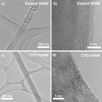 |
| Transmission electron micrographs (TEM) of etched and CVD silicon nanowires (SiNWs). (a) & (c) TEM pictures show the overall morphology of etched SiNW and CVD SiNW. (b) & (d) High-resolution TEM pictures show the surface properties of etched SiNW and CVD SiNW. (Reprinted with permission from Wiley-VCH Verlag) |
| In order to answer experimentally whether the nanowire morphology is intrinsically disadvantaged (compared to microwires and bulk), the Boston College team compared three types of samples: planar silicon wafers, silicon nanowires prepared by electroless etching, and silicon nanowires synthesized by a bottom-up chemical method. |
| "Derived from planar silicon crystals, electroless etched silicon nanowires have the same crystallography and doping level as silicon crystals from the bulk, they differ only in the surface-to-volume ratio," explains Wang. "Studying electroless etched silicon nanowires allows the collection of quantitative information on their performance and to relate this information to the nanowire morphology." |
| In their experiment, the team measured an energy conversion efficiency of 12.8% for devices using planar silicon and 10.1% for electroless etched silicon nanowire-based devices. |
| According to Wang, this result is significant in two respects: "Firstly, the measured efficiency is among the highest reported for silicon nanowires generated by any preparation method. Secondly, the outstanding performance highlights the potential of nanowires." |
| He points out that, by stark contrast, extremely modest efficiencies were measured on chemically grown silicon nanowires, the efficiencies being two orders of magnitude lower than those of electroless etched silicon nanowires. |
| "Our result raises the question as to what limits the performance of chemically grown silicon nanowires for energy conversion" says Wang. "We therefore compare microstructures of electroless etched silicon nanowires and chemically grown ones to each other. Evidentially, silicon nanowires made by these two methods show a remarkable resemblance in morphology, dimension, crystallinity, and doping level. As such, we conclude that the nanowire morphology is not intrinsically disadvantaged as far as the photovoltaic application is concerned." |
| This result requires that detailed studies of charge behavior within silicon nanowires made by different methods are necessary to understand the origin of the poor performance by chemically grown ones. |
| The researchers chose a powerful analytical method – electrochemical impedance spectroscopy (EIS) – which is often used in characterizing battery electrodes. In essence, EIS studies the system response to the application of a periodic small amplitude alternating current (AC) signal. |
| They found that experiments on electroless etched silicon nanowires on one hand and chemically grown ones on the other, returned drastically different results. |
| "Firstly" says Wang, "in the low-frequency region, the impedance of chemically grown silicon nanowires is approximately 10 times lower than that of electroless etched ones. Secondly, with increasing frequencies, we find significant differences in the decrease of impedance, suggesting that charge-transfer channels other than that through the space-charge region and the surface states exist; these channels seriously undermine the capacitive nature of the space-charge region." |
| "Although the exact nature and the origin of the additional states are unclear, it is the first time that such states have been quasi-quantitatively identified" continues Wang. "As the effects of similar defects are not observed on silicon nanowires of comparable dimension, crystallinity, and doping level, but different preparation technique (electroless etching), we hypothesize that this type of defects result from the synthetic step." |
| This understanding is particularly important, given the widely varying conditions for silicon nanowire preparation. At the heart of the problem is that it matters how materials such as silicon nanowires are synthesized. The research by Wang's team unambiguously points to this understanding. |
| "Our key observation is that nanowire morphology deserves significant research attention and that the focus should be on growth chemistry," says Wang. "We also emphasize that the performance of silicon nanowires for solar energy conversion needs to be cautiously compared by taking into account the preparation methods; otherwise misleading conclusions may be drawn." |
 By
Michael
Berger
– Michael is author of four books by the Royal Society of Chemistry:
Nano-Society: Pushing the Boundaries of Technology (2009),
Nanotechnology: The Future is Tiny (2016),
Nanoengineering: The Skills and Tools Making Technology Invisible (2019), and
Waste not! How Nanotechnologies Can Increase Efficiencies Throughout Society (2025)
Copyright ©
Nanowerk LLC
By
Michael
Berger
– Michael is author of four books by the Royal Society of Chemistry:
Nano-Society: Pushing the Boundaries of Technology (2009),
Nanotechnology: The Future is Tiny (2016),
Nanoengineering: The Skills and Tools Making Technology Invisible (2019), and
Waste not! How Nanotechnologies Can Increase Efficiencies Throughout Society (2025)
Copyright ©
Nanowerk LLC
|

Become a Spotlight guest author! Join our large and growing group of guest contributors. Have you just published a scientific paper or have other exciting developments to share with the nanotechnology community? Here is how to publish on nanowerk.com. |
