| Posted: Mar 23, 2011 |
Novel 3D sculpturing of photonic crystals promises functionality at visible wavelengths |
| (Nanowerk Spotlight) Photonic crystals – also known as photonic band gap material – are similar to semiconductors, only that the electrons are replaced by photons (i.e. light). By creating periodic structures out of materials with contrast in their dielectric constants, it becomes possible to guide the flow of light through the photonic crystals in a way similar to how electrons are directed through doped regions of semiconductors. The photonic band gap (that forbids propagation of a certain frequency range of light) gives rise to distinct optical phenomena and enables one to control light with amazing facility and produce effects that are impossible with conventional optics. |
| Photonic crystals are used to guide and localize light for all-optical processing of signals/information; to engineer dispersion and slow light; to harvest light (collect and redirect); and thresholdless lasing, that can be engineered by setting spectral ranges where light can be emitted. |
| The concept of photonic crystals was introduced in 1987 with two milestone papers by Eli Yablonovitch ("Inhibited Spontaneous Emission in Solid-State Physics and Electronics") and Sajeev John ("Strong localization of photons in certain disordered dielectric superlattices"). |
| "Control of light absorption and emission by engineering photon density of states via periodic modifications of dielectric properties of material is at the core of a photonic crystal concept," Saulius Juodkazis, Professor of Nanophotonics at Swinburne University of Technology, explains to Nanowerk. "However, as we are moving into nanoscale dimensions, technical challenges are mounting for three-dimensional (3D) structuring of materials." |
| He notes that lithography-based approaches rely on 2D processing and usually require multistep procedures for the fabrication of 3D micro- and nanoscale objects. At this range, it becomes increasingly difficult to fulfill high tolerances required for fabrication of photonic crystals operational at the visible spectral range. |
| Juodkazis points out that, so far, there have been no demonstrations of full photonic bandgap at visible wavelengths – i.e., that at a certain visible range (between 400 nm to 780 nm) determined by the 3D photonic crystal structure, the light is rejected (reflected) at all angles of incidence. |
| "In nature" he says, "opals and butterfly wings are probably the most known examples of larger area/volume structures where a 3D arrangement of materials with feature size of 100-200 nm delivers control over green-red visible spectral range. Yet this remains a challenging task for modern technology." |
| He adds that the ideal photonic crystal functional in visible spectral range should be made out of crystal (lesser losses due to scattering and absorption as compared with amorphous materials), be of a high refractive index (usually >2), and have the required 3D ordered structure of high porosity (about 70%). |
| In a paper in the March 14, 2011 edition of Optics Express ("Sculpturing of photonic crystals by ion beam lithography: towards complete photonic bandgap at visible wavelengths"), first-authored by Juodkazis and in collaboration with Prof. Sajeev John and his team, as well as ion beam lithography experts from Raith Gmbh, the team demonstrates a new approach of 3D nanostructuring by tightly focused (∼ 10nm) gallium ion beam. |
| In their work, the researchers fabricated a slanted-pore photonic crystal structure by drilling holes into a rutile-titania crystal. The period of the structure is 260 nm and the aspect ratio of 100 nm-diameter pores reached 8-10. |
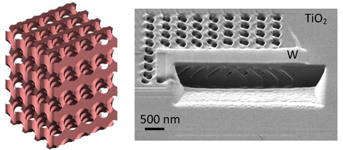 |
| Left: Design of the photonic crystal structure. Right: Scanning ion microscopy image of the focused ion beam cross section of the fabricated photonic crystal structure. (Image: Saulius Juodkazis, Swinburne University of Technology) |
| The direct 3D nano-sculpturing process used by the team does not require any special sample treatment – just a standard anti-charging coating – nor any time consuming lithographic steps. |
| "Current fabrication methods of 3D photonic crystals are using multi-step lithographical processing, direct laser polymerization, infiltration for inversion into high refractive index materials, etc." says Juodkazis. "All those approaches are laboratory demonstrations rather than development of new practical solutions. Our motivation is to show a new and efficient method to make 3D photonic crystal out of crystal." |
| The ion beam direct writing approach demonstrated in this work has implications for potential large-scale, industrial uses: 3D structures can be made on-chip, mechanically manipulated on site, and be integrated into optical circuits. Specifically, since the 3D photonic crystal is made out of the required material, e.g. titania, it can be cut out from its fabrication location and put into a required location using ion-cutting/deposition functionality of the same ion-beam setup (although this step has yet to be tested, the technical ability is present). |
| The team notes that ion beam setups are widely used to cut and section samples for transmission electron microscopy by attaching them to handling rods by ion deposition. By the same method, a 3D photonic crystal can be made, cut out, and positioned into a functional location. So far, in photonic crystal fabrication, performing these steps has not been possible with a single approach. |
| "The great potential of 3D photonic crystal lies in the possibility to control light on a sub-wavelength scale," explains Juodkazis. "This should provide opportunities to connect 3D ion sculpturing with plasmonics – light confined into 2D and 3D metallic structures – and atomic layer deposition which can be used to deposit atomic layers on 3D nanostructures." |
| He adds that light extraction from solid state lighting devices (e.g., light emitting diodes) and a reciprocal task to harvest light for solar cell applications could all be seen as beneficiaries of this 3D nano-sculpturing approach. Also, new lasing and light-emitting micro devices could use these nano-patterned 3D photonic crystals to control light emission and flow. |
 By
Michael
Berger
– Michael is author of four books by the Royal Society of Chemistry:
Nano-Society: Pushing the Boundaries of Technology (2009),
Nanotechnology: The Future is Tiny (2016),
Nanoengineering: The Skills and Tools Making Technology Invisible (2019), and
Waste not! How Nanotechnologies Can Increase Efficiencies Throughout Society (2025)
Copyright ©
Nanowerk LLC
By
Michael
Berger
– Michael is author of four books by the Royal Society of Chemistry:
Nano-Society: Pushing the Boundaries of Technology (2009),
Nanotechnology: The Future is Tiny (2016),
Nanoengineering: The Skills and Tools Making Technology Invisible (2019), and
Waste not! How Nanotechnologies Can Increase Efficiencies Throughout Society (2025)
Copyright ©
Nanowerk LLC
|

Become a Spotlight guest author! Join our large and growing group of guest contributors. Have you just published a scientific paper or have other exciting developments to share with the nanotechnology community? Here is how to publish on nanowerk.com. |
