| Posted: Jul 26, 2011 |
Integrating DNA nanotechnology with traditional silicon processing for sub-20nm resolution |
| (Nanowerk Spotlight) To build microprocessors with more than one billion transistors, manufacturers still use the same technique – photolithography, the high-tech, nanoscale version of printing technology – that they have been using for the past 50 years. State-of-the-art photolithography processes use 193 nm light to produce diffraction-limited features as small as 32 nm. |
| Going beyond 32 nm, the cost and complexity rises significantly, posing massive technological and economic challenges for chip manufacturers. This provides plenty of incentives for researchers to explore alternative manufacturing technologies for chipmakers, for instance with electron-beam lithography (see: "The future of chip manufacturing"). |
| Another novel approach, that just has been reported in the July 13, 2011 online issue of Journal of the American Chemical Society ("Molecular Lithography through DNA-Mediated Etching and Masking of SiO2"), is based on the use of DNA nanostructures to pattern a silicon wafer. |
| This work is the first to directly transfer the shape of DNA nanostructure to SiO2, making it possible to integrate DNA nanotechnology with traditional silicon processing. |
| "Our approach to pattern transfer for bottom-up nanofabrication is based on the discovery that DNA promotes/inhibits the etching of SiO2 at the single-molecule level, resulting in negative/positive tone pattern transfers from DNA to the SiO2 substrate," Haitao Liu, an assistant professor in the Department of Chemistry at the University of Pittsburgh, explains to Nanowerk. "DNA nanostructures can be made with precise control over their sizes and shapes. Their use as lithography mask, however, has been limited due to their poor chemical stability. Our work provides a way to transfer the shape of the DNA nanostructure to silicon wafer, with sub-20 nm resolution." |
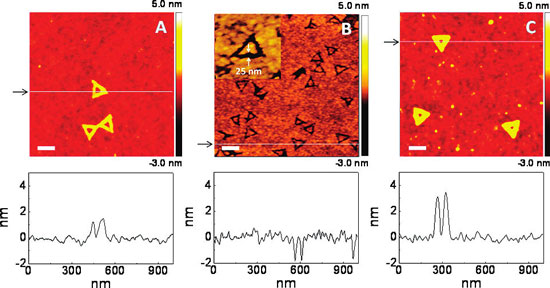 |
| (top) AFM images and (bottom) cross sections: (A) Triangular DNA origami on a SiO2 surface. (B) Triangular trenches produced upon exposure of (A) to HF vapor under high-moisture conditions. The inset shows a high-magnification AFM image of a triangular trench with a width of 25 nm. (C) Triangular ridges produced upon exposure of (A) to HF vapor under low-moisture conditions. Arrows indicate the lines along which the cross sections were determined. Scale bars represent 100 nm. (Reprinted with permission from American Chemical Society) |
| The still unoptimized conditions employed by Liu's team routinely produce 20 nm wide trenches, which may be useful as nanofluidic channels. This method, if applied to a much thinner SiO2 film, would produce a patterned SiO2 layer that could be used as a mask for etching of the underlying silicon substrate. |
| "We believe that this methodology will open up new opportunities in using self-assembled soft materials as templates for bottom-up nanofabrication, with the possibility of achieving molecular-scale resolution" says Liu. |
| For their experiments, the Pitt team deposited triangular DNA origami onto a silicon wafer having a 300 nm layer of silicon oxide. The etching of SiO2 was carried out by exposing the substrate to HF gas inside a custom-built chamber. After the etching, the silicon substrate was rinsed to remove the DNA. |
| AFM images (see figure above) of the cleaned wafer surface show triangular-shaped trenches resembling the shape of the DNA origami. |
| "The formation of the trench indicates that the DNA origami locally increases the rate of oxide etching under these conditions" explains Liu. "The full width at half-maximum of the trench (16.7 ± 2.8 nm) is comparable with the edge width of the DNA origami, indicating an overall faithful pattern transfer process. This result is consistent with our hypothesis that DNA can increase the etching rate of SiO2 by increasing the concentration of water. The small width of the trench shows that this effect is indeed spatially localized around the DNA." |
| The researchers point out that the relative humidity may play an important role in this reaction. They found that at low relative humidity, the DNA nanostructure slows the etching of the underlying SiO2, resulting in a positive tone pattern transfer from the DNA to the substrate. |
| "On the basis of our analysis, we expect DNA to increase or decrease the etching rate of SiO2 depending on the relative humidity of the environment" says Liu. |
| The team is now attempting to fabricate sub-10 nm features by depositing DNA nanostructure onto silicon wafer. The major challenges in this undertaking are the issue of how to further increase the contrast of the transferred pattern and, crucially, to increase fidelity, consistency and accuracy of the process. |
 By
Michael
Berger
– Michael is author of four books by the Royal Society of Chemistry:
Nano-Society: Pushing the Boundaries of Technology (2009),
Nanotechnology: The Future is Tiny (2016),
Nanoengineering: The Skills and Tools Making Technology Invisible (2019), and
Waste not! How Nanotechnologies Can Increase Efficiencies Throughout Society (2025)
Copyright ©
Nanowerk LLC
By
Michael
Berger
– Michael is author of four books by the Royal Society of Chemistry:
Nano-Society: Pushing the Boundaries of Technology (2009),
Nanotechnology: The Future is Tiny (2016),
Nanoengineering: The Skills and Tools Making Technology Invisible (2019), and
Waste not! How Nanotechnologies Can Increase Efficiencies Throughout Society (2025)
Copyright ©
Nanowerk LLC
|

Become a Spotlight guest author! Join our large and growing group of guest contributors. Have you just published a scientific paper or have other exciting developments to share with the nanotechnology community? Here is how to publish on nanowerk.com. |
