| Posted: Aug 30, 2011 |
Probing the molecular world with nanolamps |
| (Nanowerk Spotlight) Most molecular probes used in biomedical research require dyes or fluorescence in order to obtain meaningful signals. These probes usually are quite limited with regard to the complexity of what they can image – be it the measurable concentration range or the number of molecules that can be simultaneously detected. This is an issue that is particularly relevant when it comes to track the simultaneous multiple molecular transformations that dictate complicated diseases like cancer. |
| Rohit Bhargava and his group at the University of Illinois have come up with an intriguing new class of molecular probes to solve this problem. They took an existing spectroscopic technique – surface-enhanced Raman scattering (SERS) – and developed a unique class of nanoparticle labels that provide for different responses when excited by laser light. |
| In the past, the spectral responses obtained by techniques like SERS and nanoparticle enhanced spectroscopy were unreliable due to a lack of a rational approach in harnessing the amplification effect. The research by Bhargava's team proposes a logical approach in providing a solution to this unreliability issue. |
| "We are in the process of demonstrating the feasibility of devising a palette of molecular labels (probes) using a template called Nano-Layered Metal-dielectric Probes (nanoLAMPs)," Anil Kodali, a researcher at the University of Illinois at Urbana Champaign, tells Nanowerk. "These probes when bound to the molecules of analytical interest can easily indicate their abundance. Several different reporters can be embedded in the nanoLAMPs, providing for an ability to obtain different spectral responses while their structure is designed such that it provides for responses at any desired magnitude." |
| Kodali is first author of two papers that demonstrate this possibility, one published in Proceedings of the National Academy of Sciences ("Optimally designed nanolayered metal-dielectric particles as probes for massively multiplexed and ultrasensitive molecular assays"), the other in Optics Express ("Optimized nanospherical layered alternating metal-dielectric probes for optical sensing"). |
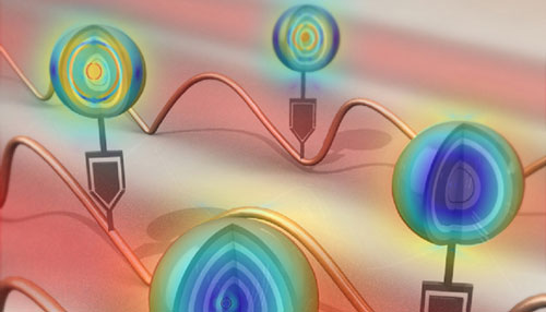 |
| Nano-Layered Metal-dielectric Particles, or nanoLAMPS for short, created by Anil Kodali, and Rohit Bhargava, along with Alex Jerez and Jeremy Miller of Beckman Institute for Advanced Science and Technology's Visualization Laboratory. The nanoLAMPs are the onion-shaped object at top, with a recognition link connecting them to the target molecule (the wavy lines) below. (Illustration: Anil Kodali, Rohit Bhargava) |
| Theoretically unlimited number of labels with different responses and at different magnitudes can be obtained with this new technique, which will facilitate imaging hundreds of molecular species quantitatively from a single molecule up to any limit. |
| "We have an almost unlimited ability with this design to put in any molecule and use it as a marker," says Bhargava. "We don't need it to be a dye or fluorescent molecule, but just need to change the molecular structure of the reporter. nanoLAMPs allows us to image any molecular species, presents many routes to fabrication, and you can put in any dye you like, any reporter, use most any metal you like." |
| The researchers say that their work will advance the existing tools for biomedical research by a great leap along with providing a fundamentally significant advance in fields like nanoparticle-based optics, SERS, analytical sensing, and optical spectroscopy. |
| According to the team, the breakthrough aspect of this new method is that it is able to overcome deficiencies found in SERS through the design of the nanoscale structure of LAMPs using classical electromagnetic theory and advanced computing strategies. |
| The nanoLAMPS were created with a unique concentric, multi-shell structure – nano-layered metal-dielectric particles – that allows for fine tuning the electric field surrounding a molecule. |
| "We applied fundamental electromagnetic theory to predict the electric field, then used algorithms and the computing power of the National Center for Supercomputing Applications (NCSA) at Illinois to optimize structures for Raman enhancement," says Kodali. |
| As they describe in the PNAS paper, the unique part of the team's design is that it completely ignores the chemical enhancement by decoupling the molecule from the surface. |
| "Instead, we embed the molecule in the dielectric layer between the metal layers" says Bhargava. "As a consequence, very, very few molecules are actually even close to the surface; they are all in the dielectric layer. That means we can completely eliminate the chemical effect and only rely on the electromagnetic effect for enhancement." |
| Going forward, the team is working on solving remaining challenges posed by the limits of fabrication approaches available to make NanoLAMPs and fixing the issues due to nonspecificity in making the structures. Another issue could also be the investigation of these structures for toxicity effects when introduced into cells for detection. |
 By
Michael
Berger
– Michael is author of four books by the Royal Society of Chemistry:
Nano-Society: Pushing the Boundaries of Technology (2009),
Nanotechnology: The Future is Tiny (2016),
Nanoengineering: The Skills and Tools Making Technology Invisible (2019), and
Waste not! How Nanotechnologies Can Increase Efficiencies Throughout Society (2025)
Copyright ©
Nanowerk LLC
By
Michael
Berger
– Michael is author of four books by the Royal Society of Chemistry:
Nano-Society: Pushing the Boundaries of Technology (2009),
Nanotechnology: The Future is Tiny (2016),
Nanoengineering: The Skills and Tools Making Technology Invisible (2019), and
Waste not! How Nanotechnologies Can Increase Efficiencies Throughout Society (2025)
Copyright ©
Nanowerk LLC
|

Become a Spotlight guest author! Join our large and growing group of guest contributors. Have you just published a scientific paper or have other exciting developments to share with the nanotechnology community? Here is how to publish on nanowerk.com. |
