| Posted: Dec 12, 2011 |
Nanofabrication made easy with cheap, homemade benchtop photolithography system |
| (Nanowerk Spotlight) Currently, the primary tool for defining patterns at the micro- and nanometer scale is the mask aligner. Even where soft lithography methods are used, mask aligners are still often required to fabricate the masters. |
| A mask aligner is a machine that is bulky in size and weight (several hundred kilograms) and is limited in the area that it can pattern in a single step (about 0.5 m2). Also, a significant amount of infrastructure is needed for operation, such as high voltage power supplies and gas cooling lines. The average cost of this tool is in the six figures (USD), which is a barrier for many labs and businesses in research and development of micro- and nanotechnologies. |
| Researchers have now developed a compact and portable photolithography system based on a solid-state light source to remove these limiting factors and, at the same time, make available the high quality patterns that a mask aligner can produce. |
| "Our solid-state photolithography system (SSP) is a low-cost (as low as $30) and compact (about 0.003 m3 and less than 1 kg) system that can be built from off-the-shelf parts and operated on the bench-top," Teri W. Odom, Board of Lady Managers of the Columbian Exposition Professor of Chemistry and Professor of Materials Science and Engineering at Northwestern University, tells Nanowerk. |
| In a previous Nanowerk Spotlight we reported on another nanofabrication technique that Odom's group improved: Revolutionizing nanofabrication with programmable nanolithography. |
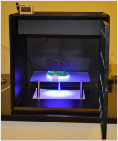 |
| The SSP system with the UV light source on. (Image: Odom Group, Northwestern University) |
| First-authored by Mark D. Huntington, a graduate student in Odom's group, a recent paper in Small ("A Portable, Benchtop Photolithography System Based on a Solid-State Light Source") describes the device that can be constructed from an array of UV light-emitting diodes (LEDs) and powered by AA batteries. |
| Given its low cost and footprint, the portable SSP has the potential to bring high-quality nanomanufacturing to every lab and small business. |
| "The array-based design of the solid-state light source alleviates the need for the sophisticated exposure optics used in mask aligners and allows the exposure area to be easily scaled," explains Huntington. "In principle, the patterning area can be increased to arbitrarily large areas simply by adding more LEDs to the array. In our work, we built and tested two systems: a 200-LED system that can be used with industry standard 4-in wafers (at a cost of $400); and a smaller system that can be used with 2-inch test wafers (at a cost of $30)." |
| Odom points out that the array-based design of the solid-state light source alleviates the need for sophisticated exposure optics used in contact mask aligners and, significantly, allows the exposure area to be easily scaled. Low energy consumption is another considerable plus: the total power consumption of the 200-LED array is less than 0.2% of the power required for the high-power mercury-vapor lamps used as light source in mask aligners for the same exposure time. In addition, GaN-based LEDs have been shown to last more than 50 times longer than mercury-vapor lamps. |
| "In combination, these factors reduce both the cost and environmental impact of nanomanufacturing," she says. "Because of its lower unit cost and reduced infrastructure requirements, SSP broadens the accessibility of micro- and nanostructures that could have an impact on a wide range of areas, such as photonics and sub-wavelength patterns, microfluidic devices and MEMS." |
| The researchers tested their SSP system using traditional photomasks as well as unconventional masks to determine capabilities and to compare against alterative photolithography methods. They found that this simple SSP system was able to create photoresist patterns with critical feature sizes around 200 nm across 4-inch wafers. |
| "Although vacuum is usually required for uniform contact between the photomask and the resist, our SSP was not designed with this feature so that complexity and cost would be reduced," says Huntington. "Thus, we simply pressed the mask into contact with the substrate, which resulted in high quality patterns over approximately 70% of the exposed area, which is about 4 cm2 in our test case." |
| Odom has high hopes for the SSP: "We anticipate that the ability of SSP to prototype a wide range of structures will accelerate the development of micro- and nanoscale devices and other applications". |
 By
Michael
Berger
– Michael is author of four books by the Royal Society of Chemistry:
Nano-Society: Pushing the Boundaries of Technology (2009),
Nanotechnology: The Future is Tiny (2016),
Nanoengineering: The Skills and Tools Making Technology Invisible (2019), and
Waste not! How Nanotechnologies Can Increase Efficiencies Throughout Society (2025)
Copyright ©
Nanowerk LLC
By
Michael
Berger
– Michael is author of four books by the Royal Society of Chemistry:
Nano-Society: Pushing the Boundaries of Technology (2009),
Nanotechnology: The Future is Tiny (2016),
Nanoengineering: The Skills and Tools Making Technology Invisible (2019), and
Waste not! How Nanotechnologies Can Increase Efficiencies Throughout Society (2025)
Copyright ©
Nanowerk LLC
|

Become a Spotlight guest author! Join our large and growing group of guest contributors. Have you just published a scientific paper or have other exciting developments to share with the nanotechnology community? Here is how to publish on nanowerk.com. |
