| Posted: Aug 27, 2007 |
Nanoelectromechanical systems start to take shape |
| (Nanowerk Spotlight) In his famous 1959 speech "Plenty of Room at the Bottom", Richard Feynman offered a prize of $1000 "to the first guy who makes an operating electric motor – a rotating electric motor which can be controlled from the outside and, not counting the lead-in wires, is only 1/64 inch cube." |
| Feynman had hoped his reward would stimulate some new fabrication technology but he was quite consternated when one year later, Bill McLellan, using amateur radio skills, built the motor with his hands using tweezers and a microscope (and many, many hours of fiddling around). McLellan's 2000 rpm motor weighed 250 micrograms and consisted of 13 parts. |
| In the almost 50 years since, not only has the field of microelectromechanical systems (MEMS) caught up with Feynman's bet and achieved commercial production capabilities of motors many times smaller than McLellan's, but researchers have begun exploring another level of miniaturization – nanoelectromechanical systems (NEMS). Efficient actuation, the creation of mechanical motion by converting various forms of energy to rotating or linear mechanical energy, is an important – and today still frustrating – issue in designing NEMS. |
| Research on building functional nanoscale electromechanical systems is well underway, as just demonstrated with another achievement by scientists at Caltech – the place where Feynman gave his speech and McLellan's motor still is on display. |
| The two principal components common to most electromechanical systems irrespective of scale are a mechanical element and transducers. The mechanical element either deflects or vibrates in response to an applied force. Depending on their type, the mechanical elements can be used to sense static or time-varying forces. The transducers in MEMS and NEMS convert mechanical energy into electrical or optical signals and vice versa. |
| To give an example, MEMS are used as accelerometers in modern automobile airbags where they sense deceleration and, if the force is beyond a programmed threshold, initiate the inflation of the airbag. |
| "NEMS have shown great promise as highly sensitive detectors of mass, displacement, charge, and energy" Prof. Michael L. Roukes explains to Nanowerk. "However, as electromechanical devices are scaled downward, transduction becomes increasingly difficult, hampering efforts to create finely controlled integrated systems. In spite of substantial progress in the field, an efficient, integrated, and customizable technique for actively driving and tuning NEMS resonators has remained elusive." |
| What NEMS researchers had found was that conventional approaches such as magnetomotive, electrostatic, and electrothermal techniques suffer from either low power efficiency, limited potential for integration, or poor nanoscale control over electromechanical coupling. |
| A new paper, first-authored by Dr. Sotiris Masmanidis, in this month's issue of Science titled "Multifunctional Nanomechanical Systems via Tunably Coupled Piezoelectric Actuation" describes how the piezoelectric effect can give rise to interesting electromechanical actuation phenomena that are only strongly manifested in NEMS. |
| Masmanidis, a researcher at California Institute of Technology's Kavli Nanoscience Institute, collaborated with Rassul Karabalin from Caltech, Iwijn De Vlaminck from IMEC in Belgium and researchers from the National Institute for Nanotechnology in Edmonton, Canada. |
| Piezoelectricity is a coupling between a material's mechanical and electrical behavior. When a piezoelectric material is squeezed, twisted, or bent, electric charges collect on its surfaces. Conversely, when a piezoelectric material is subjected to a voltage drop, it mechanically deforms. Many crystalline materials exhibit piezoelectric behavior and when such a crystal is mechanically deformed, the positive- and negative-charge centers are displaced with respect to each other. |
| "The traditional view calls for well-defined, alternating layers of electrodes and piezoelectric materials" says Masmanidis. "But this view breaks down in nanoscale devices made from semiconductors, where charge depletion smears out the boundary between piezoelectrically inactive (electrically conducting) and active (electrically insulating) regions. This effect is only significant when the total device thickness approaches the semiconductor?s charge depletion width." |
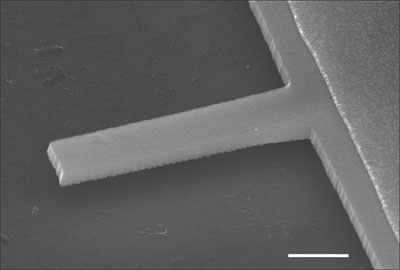 |
| NEMS cantilever used to explore depletion-mediated actuation. The scale bar is 1 micrometer. Dimensions are: Length = 4 µm, Width = 0.8 µm, Thickness = 0.2 µm. The structure consists of three layers of gallium arsenide arranged vertically in a p-type/intrinsic/n-type diode configuration. (Image: Dr. Michael L. Roukes) |
| To demonstrate the concept of depletion-mediated NEMS actuation the team around the Caltech researchers, led by Roukes, fabricated cantilevers and doubly clamped beams out of a 200 nm thick diode consisting of gallium arsenide. The piezoelectric effect inherent to this material afforded a highly efficient means of resonantly exciting these devices with an alternating voltage. |
| "Our experiments revealed that the efficiency of driving the devices can be tuned with DC voltage, as well as by tailoring the doping profile of the diode" says Masmanidis. "This novel form of control offers a new paradigm in designing NEMS." |
| Besides depletion-mediated actuation, the team demonstrated some additional functionality with these devices. One remarkable feature of NEMS fabricated from piezoelectric materials is voltage-induced resonance-frequency control; another a nanomechanical logic element based on the crystallographic anisotropy of piezoelectricity. "The integration of a reliable and customizable frequency-tuning method adds a useful layer of functionality that has so far been absent in NEMS" says Roukes. |
| Masmanidis points out that the electromechanical coupling phenomena of their device relies entirely on intrinsic material properties. This should facilitate the creation of compact, tunable NEMS arrays for applications ranging from mass and charge detection for chemical species sensing, high speed and low power switches, to nanomechanical logic gates for new computational paradigms. In particular the ability to regulate actuation efficiency through depletion-mediated strain in the semiconductor heterostructure?s low?operating-power regime raises the prospect for developing efficient, high-speed electromechanical switches. |
| "In principle, the reversibility of piezoelectric phenomena also offers the potential for ultrasensitive electrical measurement of nanomechanical motion" says Roukes. "Finally, all the concepts we presented are transferable to a wide variety of other materials beyond gallium arsenide (such as aluminum nitride, silicon carbide, or zinc oxide), which may provide enhanced electrical and mechanical properties." |
 By
Michael
Berger
– Michael is author of four books by the Royal Society of Chemistry:
Nano-Society: Pushing the Boundaries of Technology (2009),
Nanotechnology: The Future is Tiny (2016),
Nanoengineering: The Skills and Tools Making Technology Invisible (2019), and
Waste not! How Nanotechnologies Can Increase Efficiencies Throughout Society (2025)
Copyright ©
Nanowerk LLC
By
Michael
Berger
– Michael is author of four books by the Royal Society of Chemistry:
Nano-Society: Pushing the Boundaries of Technology (2009),
Nanotechnology: The Future is Tiny (2016),
Nanoengineering: The Skills and Tools Making Technology Invisible (2019), and
Waste not! How Nanotechnologies Can Increase Efficiencies Throughout Society (2025)
Copyright ©
Nanowerk LLC
|

Become a Spotlight guest author! Join our large and growing group of guest contributors. Have you just published a scientific paper or have other exciting developments to share with the nanotechnology community? Here is how to publish on nanowerk.com.
