| Posted: Mar 27, 2012 |
Move over chips - here come multifunctional labs on a single fiber |
| (Nanowerk Spotlight) Optical fibers have revolutionized telecommunications by providing higher performance, more reliable telecommunication links with ever decreasing bandwidth cost. Optoelectronic and fiber optic components are now manufactured on a large scale and the world is interconnected by an information superhighway built of glass. |
| In parallel with these developments, fiber-optic sensor technology has been a major user of technologies associated with the optoelectronic and fiber optic communications industry. Today, with the rapid advance of communications and especially sensing applications, there is an ever increasing need for advanced performance and additional functionalities. This, however, is difficult to achieve without addressing fundamental fabrication issues related to the integration onto optical fibers of advanced functional materials at the micro- and nanoscale. |
| The key aspect of suitable fabrication methodologies for lab-on-fiber devices is to adapt all the standard fabrication processes and tools in terms of material deposition (spin coating, dip coating, sputtering, evaporation, etc.) and sub-wavelength patterning and post-processing (FIB, EBL, RIE, etc.) to operate on the tip of an optical fiber. However this approach is not straightforward since spin coating and etching procedures are very challenging when operating on such a substrate. |
| Solving these technical problems, however, will open up the possibility of developing multifunctional labs integrated onto a single optical fiber, exchanging information and combining sensorial data. This could result in auto diagnostic features as well as new photonic and electro-optic functionalities useful in many strategic sectors such as optical processing, environment, life science, safety and security. |
| "The realization of highly integrated optical fiber devices requires that several micro-and nanostructures be fabricated, embedded, and connected in order to achieve the necessary light-matter interaction and physical connection," Andrea Cusano, a researcher in the Optoelectronic Division of the Department of Engineering at the University of Sannio in Italy, explains to Nanowerk. "As a consequence, a critical issue to be addressed consists in the definition of a reliable fabrication procedure able to integrate and process – at micro- and nanoscales – several materials with the desired physical, mechanical, magnetic, chemical, and biological properties onto unconventional substrates such as the optical fiber tip. |
| Cusano, together with Emanuela Esposito from the Istituto di Cibernetica "E. Caianiello", lead a team that is working on the development of "lab-on-fiber" technology, i.e. multifunctional optical nanoprobes within a single optical fiber. |
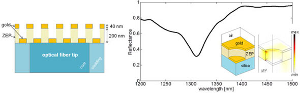 |
| Left: Schematic (cross section view) of the hybrid metallo-dielectric structure integrated on the optical fiber tip (not in scale). Right: 3D view of 1/4 of unit cell and measured reflectivity of hybrid metallo-dilectric structures characterized by a period a = 900 nm (black curve). (Reprinted with permission from American Chemical Society) |
| Lab-on-fiber technology will allow the implementation of sophisticated, autonomous multifunction sensing and actuating systems – all integrated in individual optical fibers. Such a technology would ensure unique advantages in terms of miniaturization, light weight, cost effectiveness, robustness and power consumption. |
| "Multifunctional labs integrated into a single optical fiber, exchanging information and combining sensorial data, could provide effective auto-diagnostic features as well as new photonic and electro-optic functionalities useful in many strategic sectors such as optical processing, environment, life science, safety and security," says Esposito. Lab-on-fiber technology would also provide the basis for the exploitation of many novel and intriguing phenomena that are at the forefront of scientific optical research, involving light manipulation phenomena and excitations of guided resonances in photonic crystals and quasi-crystals, as well as combined plasmonic and photonic effects in hybrid metallo-dielectric structures." |
| In a paper in the March 8, 2012 online edition of ACS Nano ("Lab-on-Fiber Technology: Toward Multifunctional Optical Nanoprobes"), the Italian research team proposes a reliable fabrication process that enables the integration of dielectric and metallic nanostructures on the tip of optical fibers, thus representing a further step in the lab-on-fiber technology roadmap. |
| "In our recent research, we propose and validate a novel fabrication process based on a 'direct writing' approach taking advantage of conventional deposition and nanopatterning techniques, typically used for planar substrates and suitably adapted to directly operate on optical fiber tip," says Cusano. |
| In essence, the team's fabrication process consists of three main technological steps: 1) dielectric overlay deposition, with flat surface and controlled thickness over the fiber core region, by means of a properly customized spin coating process; 2) nanoscale patterning of the deposited overlay by an electron-beam lithography (EBL) tool; and 3) superstrate overlay deposition, where different functional materials – metallic or non-metallic – can be deposited by various techniques (e.g. sputtering, thermal evaporation etc?), properly customized to operate with optical fibers. |
| As the researchers point out, a distinguished feature of this process is the use of a customized spin-coater chuck which allows a flat and reproducible resist layer deposited onto optical fiber tips; onto which then nanostructured arrays are directly written using an EBL system. Importantly, this fabrication process follows almost ordinary lithographic techniques – here adapted to operate on fiber facets – allowing rapid prototyping with a 90% yield and the ability to produce robust and reusable devices. |
| To demonstrate the effectiveness of their proposed methodology, the team fabricated a miniaturized fiber tip device based on a 2D hybrid metallo-dielectric nanostructure supporting localized surface plasmon resonances (LSPR). |
| "We carried out both experimental and full-wave numerical analyses to characterize the resonant phenomena" says Cusano. "The measured Q-factors were higher than those observed in typical plasmonic crystal configurations. We have also shown that the LSPR can be easily tuned by adjusting the physical and geometrical parameters of the crystal nanostructure and can be designed to be very sensitive to modifications of the surrounding medium." |
| With a view towards possible applications, the researchers have also shown some preliminary results on the capability of their platform to be used for label-free chemical and biological sensing. |
| "Moreover, we have also shown the surprising capability of our device to detect acoustic waves, taking advantage of the low elastic modulus of the patterned polymer" notes Cusano. |
| The research team, driven by the enormous potentiality of lab-on-fiber technology, is devoting their efforts to optimizing the fabrication process in terms of reliability and throughput as well as enlarging the set of functional materials to be integrated. |
| "Our dream is to get this technology to a point where it can compete with the already better established lab-on-chip technology – especially taking advantage of the higher versatility in integrating complex lighting systems as well as sophisticated optoelectronics components, devices and systems," says Cusano. |
 By
Michael
Berger
– Michael is author of four books by the Royal Society of Chemistry:
Nano-Society: Pushing the Boundaries of Technology (2009),
Nanotechnology: The Future is Tiny (2016),
Nanoengineering: The Skills and Tools Making Technology Invisible (2019), and
Waste not! How Nanotechnologies Can Increase Efficiencies Throughout Society (2025)
Copyright ©
Nanowerk LLC
By
Michael
Berger
– Michael is author of four books by the Royal Society of Chemistry:
Nano-Society: Pushing the Boundaries of Technology (2009),
Nanotechnology: The Future is Tiny (2016),
Nanoengineering: The Skills and Tools Making Technology Invisible (2019), and
Waste not! How Nanotechnologies Can Increase Efficiencies Throughout Society (2025)
Copyright ©
Nanowerk LLC
|

Become a Spotlight guest author! Join our large and growing group of guest contributors. Have you just published a scientific paper or have other exciting developments to share with the nanotechnology community? Here is how to publish on nanowerk.com. |
