| Posted: Sep 05, 2007 |
Gutenberg's grandchildren in nanotechnology labs |
| (Nanowerk Spotlight) When Gutenberg built his printing machine with moveable type in the mid 15th century, little idea did he have that he started the information age; even less that scientists would adopt the process to the nanoscale. The printing press went through several revolutionary improvements such as Lanston's monotype machine (1884), Mergenthaler's linotype machine (1886), the photo-typesetting process developed in the 1960s and finally digital printing in the 1980s. |
| Today, printing is the most widespread technology to deposit small particles onto various surfaces. Commercial desktop laser printers use toner particles with a few microns in size while top of the line high-priced industrial printing machines sometimes already use sub-micron size particles. On the other hand, the precise positioning of nanoparticles on surfaces is key to most nanotechnology applications especially nanoelectronics. However, for automated patterning of particles, existing methods are either slow (e.g., dip-pen lithography) or require prefabricated patterns on the target substrate (e.g. for electrostatic positioning). |
| Using a process akin to the printing press, researchers already have managed to bypass the need for epitaxial growth or wafer bonding to integrate wide ranging classes of dissimilar semiconducting nanomaterials onto substrates for the purpose of constructing heterogeneous, three dimensional electronics (see our Spotlight Gutenberg + nanotechnology = printable electronics). Scientist in Switzerland have now developed a parallel method for the assembly and integration of a large number of bulk-synthesized nanoparticles onto an unstructured surface with high resolution and yield. |
| "In the process we developed, discrete nanoparticles are arranged deterministically on structured surfaces using ‘directed assembly’" Dr. Heiko Wolf explains to Nanowerk. "In contrast to conventional inking, directed assembly does not merely fill predefined structures with randomly dispersed pigment particles, but arranges nanoparticles at positions that are defined by the geometry of a template. These (silicone) templates are molded with total areas in the order of 1 cm2 from hard masters with feature dimensions between 40 nm and tens of micrometers." |
| Wolf, a researcher in the Self-assembly, Nanopatterning and Soft Lithography group at IBM's Research Laboratory near Zurich, Switzerland together with IBM colleagues and scientists at ETH Zurich (led by Prof. Nicholas D. Spencer, Director of the Materials Research Center), has developed an efficient process to fabricate lines, arrays and complex arrangements of nanoparticles with high accuracy and single-particle resolution that retains individual particle functionality ("Nanoparticle printing with single-particle resolution"). |
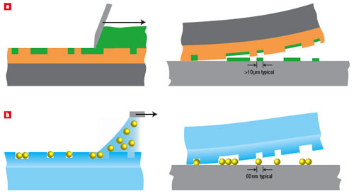 |
From traditional gravure printing to high-resolution particle printing. a, In gravure printing, a doctor blade fills the recessed features of a printing plate with ink. Pigment particles are randomly dispersed in the ink, which is transferred from the plate onto the substrate. b, In high-resolution particle printing, a selfassembly process controls the arrangement of nanoparticles on the printing plate. The entire assembly is printed onto the substrate, whereby the particle positions are precisely retained at a resolution that is three orders of magnitude higher than in conventional printing. (Reprinted with permission from Nature Publishing Group) |
| "Our printing approach is compatible with different particles, including not only metals, but also polymers, semiconductors and oxides" says Wolf. "It can handle bulk-synthesized particles directly in their original colloidal state even when they have been modified with functional molecules. Thanks to its high resolution, nanoparticle printing can efficiently define the critical dimensions for nanoscale devices." |
| In their initial experiments, the Swiss team adopted template geometries that include lines, producing close-packed nanoparticle wires as used in molecular electronics, spaced regular arrays for nanowire growth and arbitrary arrangements, such as the sun designed by the seventeenth-century alchemist Robert Fludd, which is composed of about 20,000 single particles. |
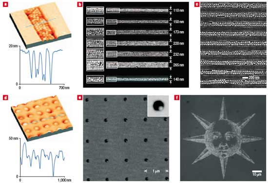 |
Particles arranged on printing plates after inking. Gold particles were assembled in poly(dimethylsiloxane) templates by hydrodynamic and surface forces. a, AFM topography and b, SEM micrographs of 60-nm Au monodispersed particles arranged in u-grooves of different widths, and one u-groove (bottom) filled with polydispersed particles. c, Larger areas of multiple, densely spaced lines have also been filled, for example 150-nm lines with 60-nm Au particles. d, AFM topography of 200-nm spaced array of 100-nm Au particles. e, 1-mm-spaced array of 60-nm Au particles. f, Bright-field optical micrograph of a sun composed of approximately 20,000 individual 60-nm Au particles. (Reprinted with permission from Nature Publishing Group) |
| In developing this novel printing process that enables the positioning of sub-100-nm particles individually and with high placement accuracy, the ETH/IBM team demonstrated their control over three key aspects: |
| 1) Accurate assembly of the nanocrystals: understanding the assembly process and designing the appropriate printing plate geometry; |
| 2) Control of the particle transport towards the assembly sites on the template: It turns out it is not sufficient to supply just enough particles – the particle concentration has to be very high, locally, to provide a high yield; |
| 3) Tuning of particle adhesion for an efficient transfer: a thin polymer layer fixes the nanocrystals on the target. |
| For printed nanoparticles to retain their useful properties during integration of course is crucial. This was shown in one of the experiments, where a surface-sensitive application was chosen to demonstrate that individual gold nanocrystals are still catalytically active after printing. |
| The new technique could be very promising for future nanoelectronics applications through the controlled placement of catalytic seed particles for the growth of semiconductor nanowires. |
| "Semiconductor nanowires are one promising route towards ultimate- and post-CMOS devices" says Wolf. "One of the great challenges there is to control the location where the nanowires are formed. By placing the catalytic seed particles in a defined position, the final position of the nanowire can be determined." |
| Wolf cautions, however, that the long-range accuracy of their method is not yet sufficient for microelectronic large-scale integration. Currently, the long-range accuracy of the new technique is similar to that of microcontact printing methods and reaches about 12 p.p.m (parts per million) average positioning errors. Reaching higher accuracies of 1 p.p.m., as required for large-scale integration in microelectronics, is a challenge that remains to be addressed. |
 By
Michael
Berger
– Michael is author of four books by the Royal Society of Chemistry:
Nano-Society: Pushing the Boundaries of Technology (2009),
Nanotechnology: The Future is Tiny (2016),
Nanoengineering: The Skills and Tools Making Technology Invisible (2019), and
Waste not! How Nanotechnologies Can Increase Efficiencies Throughout Society (2025)
Copyright ©
Nanowerk LLC
By
Michael
Berger
– Michael is author of four books by the Royal Society of Chemistry:
Nano-Society: Pushing the Boundaries of Technology (2009),
Nanotechnology: The Future is Tiny (2016),
Nanoengineering: The Skills and Tools Making Technology Invisible (2019), and
Waste not! How Nanotechnologies Can Increase Efficiencies Throughout Society (2025)
Copyright ©
Nanowerk LLC
|

Become a Spotlight guest author! Join our large and growing group of guest contributors. Have you just published a scientific paper or have other exciting developments to share with the nanotechnology community? Here is how to publish on nanowerk.com. |
