| Posted: Apr 03, 2012 |
Researchers succeed in achieving high-contrast superlens lithography |
| (Nanowerk Spotlight) The concept of a 'superlens' has attracted significant research interest in the imaging and photolithography fields since the concept was proposed back in 2000 (see the original paper by Pendry in Physical Review Letters: "Negative Refraction Makes a Perfect Lens"). A superlens would allow you to view objects much smaller than the roughly 200 nanometers that a regular optical lens with visible light would permit. This theoretical resolution limit (diffraction limit) of conventional optical imaging methodology was the primary factor motivating the development of higher-resolution scanning probe techniques. Though scanning electron microscopes can capture objects that are much smaller, down to the single nanometer range, they are expensive, heavy, and, at the size of a large desk, not very portable. |
| "Since superlenses have demonstrated the capability of subdiffraction-limit imaging, they have been envisioned as a promising technology for potential nanophotolithography," Dr. Hong Liu, a scientists in the Patterning & Fabrication Group at A*STAR's Institute of Materials Research and Engineering (IMRE), tells Nanowerk. "Unfortunately, all the experimentally demonstrated photoresist patterns exhibited very low profile depths, leading to poor contrasts, which are far below industrial requirements." |
| This bad performance of existing superlenses prevents their practical application in superlens lithography for industries such as data storage and photolithography. In fact, all plasmonic nanolithography techniques suffer from inadequate contrast. |
| In a new paper in a recent edition of Nano Letters ("High Aspect Subdiffraction-Limit Photolithography via a Silver Superlens"), first-authored by Liu, the IMRE team, led by Dr. Jinghua Teng, the Program Manager of the A*STAR Metamaterials Program and currently leading the Superlens Project, experimentally demonstrates sub-50 nm resolution nanophotolithography by using a smooth silver superlens under 365 nm UV light in a conventional photolithography setup. |
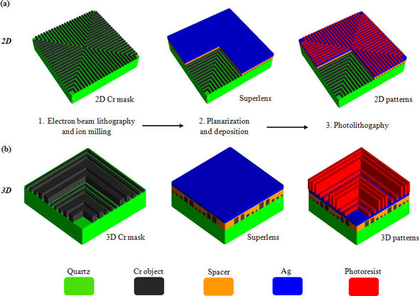 |
| Schematics of three main fabrication steps of subdiffraction-limit nanolithography using Superlens. (a) The 2D scheme to transfer the L-shape, 100 nm pitch, and 40 nm thick Cr grating patterns into photoresist. (b) The 3D scheme to transfer the 700 nm pitch gratings with linewidths varied from 55 to 135 nm in a step of 20 nm separated by a constant gap of 45 nm into photoresist. (Reprinted with permission from American Chemical Society) |
| The superlens concept relies on the generation of surface plasmon polaritons enhancing the evanescent fields to restore the near-field components of the Fourier decomposition of the source object, hence breaking the diffraction limit. |
| "We studied the factors affecting superlens performance and picked out one critical factor: the surface roughness induced scattering loss," Liu explains. "By fabricating a smooth silver superlens with nanoscale roughness, we achieved unprecedented high-contrast imaging with 45-nm resolution and high pattern fidelity ratio." |
| In addition, the researchers also achieved 3-dimensional nanopatterning in conjunction with gray scale lithography. |
| This work verifies, for the first time, that superlens-based photolithography is possible at a contrast level required by industrial manufacturing processes. |
| "We have put great effort into finding a way to circumvent the challenging superlens issue in terms of loss reduction," notes Teng. "Silver normally exhibits rough surface structures when deposited by conventional fabrication methods, leading to significant scattering loss for nanoscale plasmonic devices and metamaterials. In this work, we have applied electron beam evaporation to deposit a silver thin-film as superlens with surface roughness of less than 2 nm, which reduces the scattering loss so as to generate this high-contrast superlens." |
| Currently, optical lithography is still the dominant fabrication technology in the semiconductor industry but it has been predicted to be close to reaching its fundamental limit at the atomic level. Meanwhile, a sharp rise in the cost of advanced lithography tools, mask making, complex process and relevant materials has become a serious economic concern for the semiconductor industry. |
| With these new results, superlens lithography – among other nanolithographic tools that are being developed – now is able to demonstrate the required sub-diffraction-limit resolution and high contrast performance required for cost-effective and high throughput nanopatterning mass production. |
| "Currently, industry utilizes state-of-the-art deep UV (193 nm wavelength) immersion lithography tools to push the half-pitch resolution to around 22 nm," says Teng. "However, the cost of these advanced tools is extremely high. In our technique, the superlens can be integrated with conventional photolithography (365 nm wavelength) systems to achieve a comparable resolution and it is potentially capable of application in large-scale mass production. It greatly reduces the equipment cost and relevant materials and process cost." |
 By
Michael
Berger
– Michael is author of four books by the Royal Society of Chemistry:
Nano-Society: Pushing the Boundaries of Technology (2009),
Nanotechnology: The Future is Tiny (2016),
Nanoengineering: The Skills and Tools Making Technology Invisible (2019), and
Waste not! How Nanotechnologies Can Increase Efficiencies Throughout Society (2025)
Copyright ©
Nanowerk LLC
By
Michael
Berger
– Michael is author of four books by the Royal Society of Chemistry:
Nano-Society: Pushing the Boundaries of Technology (2009),
Nanotechnology: The Future is Tiny (2016),
Nanoengineering: The Skills and Tools Making Technology Invisible (2019), and
Waste not! How Nanotechnologies Can Increase Efficiencies Throughout Society (2025)
Copyright ©
Nanowerk LLC
|

Become a Spotlight guest author! Join our large and growing group of guest contributors. Have you just published a scientific paper or have other exciting developments to share with the nanotechnology community? Here is how to publish on nanowerk.com. |
