| Posted: Feb 09, 2006 |
New research advances the integration of hybrid organic-inorganic materials into molecular devices |
| (Nanowerk News) A group of researchers from Bell Labs, Rutgers Dept. of Chemistry, Stanford's Dept. of Chemical Engineering and the University of Konstanz's Dept. of Physics conducted the first experimental research that systematically correlates the electrical properties of SAM (self-assembled molecular layers) based molecular devices with the microscopic details of the metal–molecule interface. They demonstrated that the generation of defects can be dramatically reduced for certain combinations of metals and molecules by changing the surface topography and growth conditions at the interface. The findings were published in the Feb. 7, 2006 online issue of Nanotechnology with the title "Control of topography, stress and diffusion at molecule–metal interfaces". |
| "Our research addresses some of the major issues that are slowing the integration of hybrid organic-inorganic materials into practical device structures" Nikolai Zhitenev of Bell Labs told Nanowerk. "The methods described in our paper substantially improve the yields in the fabrication of devices with molecular monolayers active channels and significantly reduce the density of defects caused by metal penetration." |
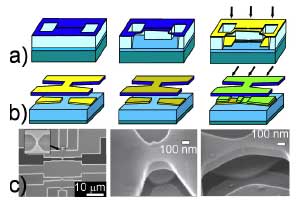 |
| Fabrication of templates and molecular junctions. a) The stencil mask is defined within an insulating stack of SiO2/Si3N4 layers grown on Si substrate. A layer of SiO2 (light blue, 10 nm in 5 µm by 5 µm central windows, 200 nm elsewhere on the wafer) is grown on Si (light purple) to isolate the substrate from the devices followed by Si3N4 (∼400 nm, cyan) and SiO2 (∼150 nm, blue) mask forming layers. The desired pattern is defined by photolithography and etching of the top SiO2 layer. Si3N4 is selectively etched undercutting the top SiO2. The mask is used to define the pattern of evaporated metal electrodes (yellow). The metal accumulated on the top surface of the mask is electrically isolated from the evaporated electrodes. b) Fabrication of molecular junction using the template. Bottom electrodes are defined on the substrate by evaporation. Molecular layer is deposited from solution. Evaporation of second electrode from an angle completes the junction. c) SEM images of the template (one out of four shown samples is shaded) and examples of small and large junctions. (Source: Bell Labs) |
| Reliable and scalable integration of organic molecules within nanoscale electronic devices has the potential to dramatically expand available device functionality. The electronic properties of molecular devices that are just a few atomic layers thick are determined not solely by the properties of the molecules but are equally dependent on dopants, defects and electronic states at the interfaces. The incorporation of molecules in small devices calls for the simultaneous solutions of many interrelated material, electronic and chemical issues. |
| The researchers studied the phenomena affecting the conductance of molecular devices by systematically varying the growth conditions at the metal-molecule interface. Transport properties of metal-molecule-metal junctions containing monolayer of conjugated and saturated molecules with characteristic dimensions in the range of 30-300 nm are correlated with microscopic topography, stress and chemical bonding at metal-molecule interfaces. Small shadow masks are used to obtain features below the usual lithographic limits. It was demonstrated that the defects/interfaces can be rationally controlled and that their properties are often more important than the electronic properties of molecules in determining the device conductance. The density of defects caused by metal penetration into monolayers is significantly reduced increasing the yield to >90%. Their statistically significant data set allowed the researchers to conclude that the conductivity of organic molecules ∼1.5 nm long is at least 4 orders of magnitude lower than is commonly believed. |
 By
Michael
Berger
– Michael is author of four books by the Royal Society of Chemistry:
Nano-Society: Pushing the Boundaries of Technology (2009),
Nanotechnology: The Future is Tiny (2016),
Nanoengineering: The Skills and Tools Making Technology Invisible (2019), and
Waste not! How Nanotechnologies Can Increase Efficiencies Throughout Society (2025)
Copyright ©
Nanowerk LLC
By
Michael
Berger
– Michael is author of four books by the Royal Society of Chemistry:
Nano-Society: Pushing the Boundaries of Technology (2009),
Nanotechnology: The Future is Tiny (2016),
Nanoengineering: The Skills and Tools Making Technology Invisible (2019), and
Waste not! How Nanotechnologies Can Increase Efficiencies Throughout Society (2025)
Copyright ©
Nanowerk LLC
|

Become a Spotlight guest author! Join our large and growing group of guest contributors. Have you just published a scientific paper or have other exciting developments to share with the nanotechnology community? Here is how to publish on nanowerk.com.
