| Posted: Oct 01, 2012 |
Making high-resolution holograms with nanoscale pixels |
| (Nanowerk Spotlight) The size of pixels is one of the key limiting features in the state of the art of holographic displays systems. Holography is a technique that enables a light field – the product of laser light scattered off objects – to be recorded and later reconstructed when the original light field is no longer present, due to the absence of the original objects. Holography can be thought of as somewhat similar to sound recording, whereby a sound field created by vibrating matter like musical instruments or vocal cords, is encoded in such a way that it can be reproduced later, without the presence of the original vibrating matter. |
| The resolution and field of view in these holographic systems are dictated by the size of the pixel, i.e. the smallest light scattering element. |
| "Light scattered from individual pixels interferes spatially to produce the projected images/diffraction patterns in holograms," Haider Butt, a post-doctoral researcher at the University of Cambridge's Centre of Molecular Materials for Photonics and Electronics (CMMPE), explains to Nanowerk. "The pixel size controls both the resolution and field of view of these projected images. Smaller pixels allow the diffraction of light at larger angles, increasing the field of view." |
| Basically this means that the smaller the pixel, the higher the resolution of the hologram. To address the limitations of current holographic systems due to their pixel size, a research team led by CMMPE's Timothy Wilkinson and Gehan Amaratunga, a professor at the University's Centre for Advanced Photonics and Electronics, set out to use nanostructures as the smallest possible light-scattering elements for producing holograms. |
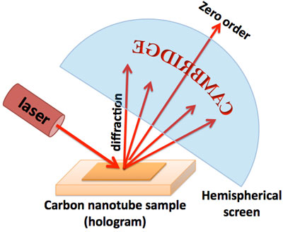 |
| The schematic diagram of the experimental setup employed to capture the diffraction pattern. (Image: Dr. Haider Butt, University of Cambridge). |
| Reporting their work in a recent issue of Advanced Materials ("Carbon Nanotube Based High Resolution Holograms"), first-authored by Butt, the scientists harnessed the extraordinary conductive and light scattering abilities of nanotubes and patterned an array of MWCNTs to produce a high resolution hologram. |
| "The fascinating aspect about our research is that we have demonstrated the utilization of carbon nanotubes as the smallest possible pixel for diffracting light in a highly controlled manner to produce a two dimensional image," says Butt. "Our objective was to control the angular diffraction from the nanotube arrays by fabricating them in the form of a holographic pattern. Such an array of subwavelength nanotubes can act as an intensity hologram (grid of apertures) towards the incident light, producing a diffraction pattern in the far field. In this manner we can replicate the mechanism of an intensity spatial light modulator while using the world's smallest pixel defined by a carbon nanotube." |
| To demonstrate the capabilities of this approach, the team calculated the holographic patterns necessary to display the word "Cambridge". They performed these calculations based on the principle of diffraction optics assuming the MWCNTs acted as diffracting elements. |
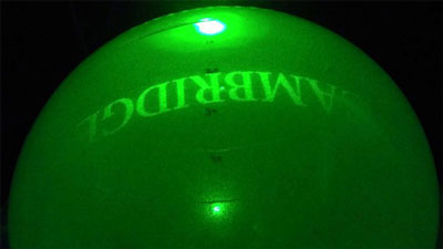 |
| The "Cambridge" pattern of the hologram. (Image: Dr. Haider Butt, University of Cambridge). |
| Based on these calculations, they then fabricated a highly ordered array of vertically aligned MWCNTs on a silicon substrate. By shining a green (532 nm) laser perpendicular to the plane of the nanotube array, a pattern with a clear "Cambridge" image was obtained on a a semitransparent hemispherical screen with a radius of 15 cm. |
| These results pave way towards the utilization of nanostructures for producing 3D holographic display systems with wide field of view and high resolution. |
| "The high resolution aspect makes these holograms very sensitive to the changes in materials properties, position and direction of incident light," Butt points out. "Based on this, a new class of highly sensitive holographic sensors can be developed that could sense distance, motion, tilt, density of biological materials, and wavefront of incident light." |
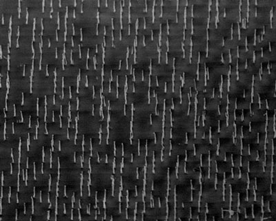 |
| SEM image of a part of the fabricated MWCNT array. (Image: Dr. Haider Butt, University of Cambridge). |
| One of the challenges for the research team is to decrease the fabrication cost of these holograms. Carbon nanotubes are still expensive materials to fabricate at large scales. In order to explore alternative materials they are now going to try zinc oxide nanowire to achieve the same effects. |
| Another challenge is to investigate movement in the projections. Currently, these nanoscale pixels can only render static holograms. "We will look at different techniques such as combining our nanotube pixels with the liquid crystals found in flat-screen technology to create fluid displays – possibly leading to changeable pictures and even razor-sharp holographic video," says Butt. |
 By
Michael
Berger
– Michael is author of four books by the Royal Society of Chemistry:
Nano-Society: Pushing the Boundaries of Technology (2009),
Nanotechnology: The Future is Tiny (2016),
Nanoengineering: The Skills and Tools Making Technology Invisible (2019), and
Waste not! How Nanotechnologies Can Increase Efficiencies Throughout Society (2025)
Copyright ©
Nanowerk LLC
By
Michael
Berger
– Michael is author of four books by the Royal Society of Chemistry:
Nano-Society: Pushing the Boundaries of Technology (2009),
Nanotechnology: The Future is Tiny (2016),
Nanoengineering: The Skills and Tools Making Technology Invisible (2019), and
Waste not! How Nanotechnologies Can Increase Efficiencies Throughout Society (2025)
Copyright ©
Nanowerk LLC
|

Become a Spotlight guest author! Join our large and growing group of guest contributors. Have you just published a scientific paper or have other exciting developments to share with the nanotechnology community? Here is how to publish on nanowerk.com. |
