| Posted: Nov 08, 2012 |
Collective states as alternative variables for information processing |
| (Nanowerk Spotlight) Power dissipation is the limiting factor to the continued scaling of size and speed of conventional silicon technology used for fabrication of integrated circuits and computer chips. For each switch of a transistor, an amount of energy needs to be dissipated that is proportional to the number of electrons and temperature. This condition is of a fundamental nature, resulting from the laws of thermodynamics. |
| "However, the assumption underlying this fundamental limit is that the electrons or spins act as an ensemble of independent particles," Alexander A. Balandin, Professor of Electrical Engineering and Founding Chair of Materials Science and Engineering at University of California - Riverside (UCR), explains to Nanowerk. "If instead, the electrons are in a collective state, then the minimum dissipation limit for one switching cycle can be greatly reduced. This fact provides a strong motivation to exploit collective states as alternative variables for information processing." |
| In conventional semiconductors, used in integrated circuits, electrons travel as independent particles. As they travel, electrons are scattered by phonons – quanta of the crystal lattice vibrations – which introduces electrical resistance. The charge density wave (CDW) is a distinguishably different quantum state where electrons and phonons are closely coupled. The charge density wave can propagate as a whole entity giving rise to the collective current. |
| The transition to this collective quantum state usually happens at a rather low temperature (about 200 K in several known materials). A research team at UCR, led by Balandin, has now proposed an application of the charge density waves for information encoding and processing. Reporting their findings in the October 23, 2012, online edition of Nano Letters & Interfaces ("Charge Density Waves in Exfoliated Films of van der Waals Materials: Evolution of Raman Spectrum in TiSe2"), they demonstrated that the transition temperature from the 'normal' to the charge-density wave state of some materials can be increased by decreasing the thickness of the materials to the nanometer-range. |
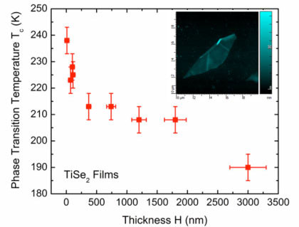 |
| Figure 1: Increase in the transition temperature in the exfoliated films of CDW materials. (The figure is courtesy of Professor Alexander A. Balandin and Pradyumna Goli, Nano-Device Laboratory, University of California - Riverside) |
| "For practical applications of CDW in information processing it is important to increase the transition temperature so that the devices implemented with CDW materials can function at room temperature of about 300 K," says Balandin. "The collective states of CDW materials that exist near room temperature are strongly preferred over those appearing only at low temperatures for a variety of technological reasons. The significance of our reported results is a demonstration that the transition temperature of CDW materials can be increased allowing for the near room-temperature operation of the devices made of such materials." |
| The researchers monitored the evolution of the transition temperature with the thickness of the film using micro-Raman spectroscopy. |
| "Transition to the CDW state is accompanied by modification of the crystal lattice structure leading to the corresponding changes in the Raman signatures of the material," notes Balandin. |
| Figure 2 below shows the Raman spectrum of the CDW material as the temperature of the sample is varied from ∼100 K to 300 K. |
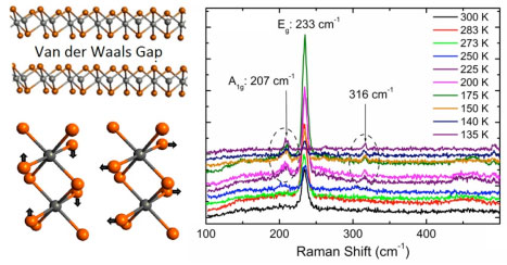 |
| Figure 2: Crystal structure of the charge density wave material (left panel) and modification of the Raman signatures of CDW film with varying temperature (right panel). One can see the appearance of new Raman peaks at the temperature near 225 K. (The figure is courtesy of Professor Alexander A. Balandin and Pradyumna Goli, Nano-Device Laboratory, University of California - Riverside) |
| For a proof-of-concept demonstration the UCR team used 'graphene-like' mechanical exfoliation of thin films of titanium diselenide. |
| "Our prior experience with graphene exfoliation was very useful" says Balandin. "We understand that any sort of practical application would require a scalable and controlled synthesis of CDW films but for initial experiments the exfoliated films worked out fine." |
| The exfoliation of TiSe2, which is a van der Waals type layered material, and Raman measurements have been carried out by Graduate Student Researcher Pradyumna Goli in Professor Balandin?s Nano-Device Laboratory (NDL) at UCR (he also is the first author of the paper). Professor Roger Lake and Graduate Student Researcher Darshana Wickramaratne provided theoretical support for this project investigating computationally the thickness dependence of the phase transition temperature in CDW films. |
| The research of the feasibility of using CDWs for information processing was funded by the National Science Foundation (NSF) and Semiconductor Research Corporation (SRC) Nanoelectronic Research Initiative (NRI) project entitled "Charge-Density-Wave Computational Fabric: New State Variables and Alternative Material Implementation" (NSF-1124733) as a part of the Nanoelectronics for 2020 and beyond (NEB-2020) program. Another investigator involved in the project – Professor John Stickney, University of Georgia – focuses on developing methods for the electrochemical atomic layer deposition of CDW films. |
| According to Balandin, for the next stages of this research, the team plans to build prototype multi-gate CDW devices and circuits in order to test the new computing paradigm, which can become possible with the CDW collective states. |
 By
Michael
Berger
– Michael is author of four books by the Royal Society of Chemistry:
Nano-Society: Pushing the Boundaries of Technology (2009),
Nanotechnology: The Future is Tiny (2016),
Nanoengineering: The Skills and Tools Making Technology Invisible (2019), and
Waste not! How Nanotechnologies Can Increase Efficiencies Throughout Society (2025)
Copyright ©
Nanowerk LLC
By
Michael
Berger
– Michael is author of four books by the Royal Society of Chemistry:
Nano-Society: Pushing the Boundaries of Technology (2009),
Nanotechnology: The Future is Tiny (2016),
Nanoengineering: The Skills and Tools Making Technology Invisible (2019), and
Waste not! How Nanotechnologies Can Increase Efficiencies Throughout Society (2025)
Copyright ©
Nanowerk LLC
|

Become a Spotlight guest author! Join our large and growing group of guest contributors. Have you just published a scientific paper or have other exciting developments to share with the nanotechnology community? Here is how to publish on nanowerk.com. |
