| Posted: Dec 11, 2012 |
Accurately determining the surface energy of solid selenium |
| (Nanowerk Spotlight) Energy-relevant materials like selenium have photovoltaic and photoconductive properties that make them interesting for the manufacture of solar cells and lighting devices, for instance as copper indium gallium selenide (CIGS) semiconductors, in cadmium-selenide quantum dots, or in more exotic variations such as bismuth-selenide topological insulators. |
| In most of these applications, as with all nanomaterials, the material surface plays a critical role. Therefore, their surface properties, and more particularly their solid surface energy – the energy required to create a new surface – have to be carefully determined in order to fully understand and control relevant manufacturing parameters for devices based on these materials. |
| A new study, reported in the December 5, 2012, online edition of Applied Physics Letters ("An accurate determination of the surface energy of solid selenium") now shows that the experimental determination of the solid surface energy of selenium is in excellent agreement with the theoretical predictions coming from nano-thermodynamics. |
| "A lower limit value of the solid surface energy of selenium (∼0.175 J/m2) has been determined in 1971 by extrapolating the surface energy of the melt of selenium at 20°C; but an attempt to determine the solid surface energy of selenium from contact angle measurements failed," Dr. Grégory Guisbiers, a senior researcher at the University of Mons in Belgium, tells Nanowerk. |
| Guisbiers and his collaborators therefore set out to experimentally determine the solid surface energy of selenium using different probe liquids in order to support the theoretical findings. |
| In the APL paper, the team now reports on the accurate determination of the solid surface energy of selenium by contact angle measurements. |
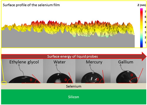 |
| The contact angles made by the different liquid probes on the selenium surface are pictured. Going from left to right, the liquid surface energy of the liquid probes increases, therefore the contact angle increases. The yellow box illustrates the surface profile of the selenium film measured by Atomic Force Microscopy. (Image: Dr. Guisbiers, University of Mons) |
| Guisbiers says that the idea to conduct this research came from nano-thermodynamics calculations: "I was investigating the size effect on the thermal expansion coefficient of selenium nanoparticles. The nano-thermodynamics model works quite well to describe the size and shape effect on other materials and properties but failed to describe the size-dependent behavior of the selenium's thermal expansion coefficient. This was strange, and I immediately suspected that the solid surface energy of selenium was wrong." |
| To conduct their experiments, the researchers used a clean room environment available at the Institute of Electronics, Microelectronics and Nanotechnology (IEMN) where temperature and humidity rate can be controlled. To achieve their objective, they used non-conventional and conventional liquids to have a wide range of liquid surface energies (0.047-0.718 J/m2). |
| "In comparison, the range of liquid surface energies used in 1971 was 0.028-0.052 J/m2" says Guisbiers. "This range failed to determine the solid surface energy of selenium since this range did not encompass the expected solid surface energy of selenium." |
| Generally, conventional probe liquids have a liquid surface energy lower than 0.1 J/m2. Using non-conventional probe liquids like mercury and gallium allows to encompass the solid surface energy of the film that should be measured. Therefore, using a wide range of liquid surface energies involving conventional and non-conventional probe liquids, the solid surface energy of the film can be determined by the sessile drop technique from contact angle measurements. |
| "The advantage of our approach is that we used nano-thermodynamics to have an idea of the solid surface energy of selenium before selecting the liquid probes," he continues. "The theoretical value has been determined to be around 0.285?0.022 J/m2. We then selected two liquids which have a lower surface energy than selenium (ethylene glycol and de-ionized water) and two liquids which have a higher surface energy compared to selenium (mercury and gallium)." |
| Being able to accurately determine the solid surface energy of selenium may benefit several application areas: For instance, it may help improve antibacterial coatings using selenium. Indeed, this may affect the ability of bacteria to adhere to selenium surfaces. |
| It may also help predict the phase diagrams of nano-alloys involving selenium. This will have an impact on the properties of selenium-based phase change materials. |
| Guisbiers points out that this work is essential for all nano-selenium structures and particularly on the surface segregation. |
| He emphasizes that, more generally, it shows one more time that nano-thermodynamics is essential to simulate correctly nanomaterial properties and it can be used as a reverse theory to improve the accuracy of bulk parameters. |
| Going forward, the team says that the determination of solid surface energy of selenium with other crystallographic orientation will be of interest. The temperature dependence of the solid surface energy of selenium has also to be determined. |
| "The nano-thermodynamic model used for the theoretical prediction can still be improved by differentiating atoms placed at edges and corners from surface atoms," says Guisbiers. "Indeed, until now, the model differentiates between bulk and surface atoms. It will be intriguing to differentiate between bulk, surface, edge and corner atoms." |
 By
Michael
Berger
– Michael is author of four books by the Royal Society of Chemistry:
Nano-Society: Pushing the Boundaries of Technology (2009),
Nanotechnology: The Future is Tiny (2016),
Nanoengineering: The Skills and Tools Making Technology Invisible (2019), and
Waste not! How Nanotechnologies Can Increase Efficiencies Throughout Society (2025)
Copyright ©
Nanowerk LLC
By
Michael
Berger
– Michael is author of four books by the Royal Society of Chemistry:
Nano-Society: Pushing the Boundaries of Technology (2009),
Nanotechnology: The Future is Tiny (2016),
Nanoengineering: The Skills and Tools Making Technology Invisible (2019), and
Waste not! How Nanotechnologies Can Increase Efficiencies Throughout Society (2025)
Copyright ©
Nanowerk LLC
|

Become a Spotlight guest author! Join our large and growing group of guest contributors. Have you just published a scientific paper or have other exciting developments to share with the nanotechnology community? Here is how to publish on nanowerk.com. |
