| Posted: Oct 16, 2007 |
Metactronics - a metamaterial-inspired nanotechnology approach towards electronics |
| (Nanowerk Spotlight) Nanoelectronics deals with functional electron devices, such as transistors, in the nanoscale range size. As the name implies, nanoelectronics runs on electricity, i.e. the transport of electrons. Another approach to creating faster,smaller and more energy-efficient electronics is to move the field of optical information processing towards the nanoscale. Optical nanoelectronics will work with light instead of electron transport. Here the usual circuit elements such as inductors, capacitors and resistors could be created in order to operate using infrared or visible light. Using nanotechnology, researchers are able to create structures that could operate on the same or smaller scale as the wavelength of light (the wavelength of visible light is roughly between 400 and 700 nanometers). Going beyond 'conventional' nanoelectronics, researchers have now proposed a form of optical circuitry in which a network of subwavelength nanoscale metamaterial structures and nanoparticles may provide a mechanism for tailoring, patterning, and manipulating optical electric fields in a subwavelength domain, leading to the possibility of optical information processing at the nanometer scale. |
| "In microelectronics, the notion of a circuit is a powerful concept in which a flow of a certain quantity – e.g., electric current as the 'flow' of charges – is related to a potential of another quantity – e.g., electric potential – through the functions of 'lumped' elements such as resistor, inductor, capacitor, and diode Dr. Nader Engheta explains to Nanowerk. "This 'lumpedness' of circuit elements is an important assumption in modeling, allowing simplification and, effectively,modularization of the function of each element. From a systems point of view, in effect what is happening inside the element becomes less relevant to the connectivity and functionality of this modularized element to the rest of the system." |
| Engheta, the H. Nedwill Ramsey Professor of Electrical and Systems Engineering, and Professor of Bioengineering at the University of Pennsylvania, therefore asked the question if this concept of lumped circuit elements, and the mathematical machinery and tools of circuit theory, can be extended and applied to the optical domain? After all, this notion of lumpedness has been extensively and successfully used in the radio frequency (RF) and microwave domains and has been proven to be a powerful tool in the design, innovation, and discovery of new functionalities in circuits in those frequency domains. |
| According to Engheta's new approach based on exploiting the optical properties of metamaterials (engineered composite materials that gain their properties from their structure rather than directly from their composition), nanoparticles may play the role of lumped nanocircuit elements such as nanoinductors, nanocapacitors, and nanoresistors, analogous to microelectronics. |
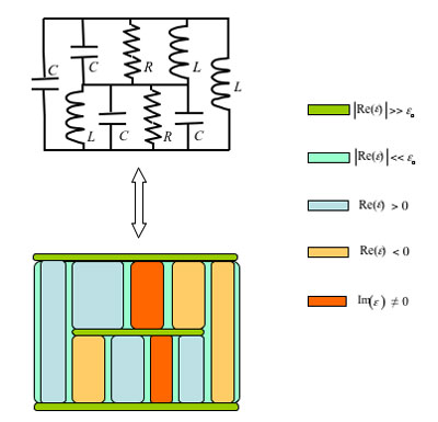 |
| Concept of optical 'metananocircuit' and metamaterial-inspired nanoelectronics – 'metactronics': A tapestry of nanostructures with different optical materials, arranged next to each other, forms an optical 'circuit', wherein optical electric fields and displacement currents are tailored in a subwavelength region, analogous to the voltages and currents in a conventional circuit. (Image: Dr. Engheta/UPenn) |
| "My idea of lumped nanocircuits with light addresses a new paradigm for optical circuitry, in which a collection of nanostructures, e.g., nanoparticles, of different materials, when arranged next to each other and when an optical signal interacts with this collection, may function as a nanoscale circuit at optical frequencies" says Engheta. "This concept can provide a new form of circuits, operating with light and at the nanoscale." |
| The Penn researcher coined the term metactronics because "indeed in this collection of nanoparticles the local optical fields can be tailored to have a desired pattern, analogous to currents and voltages in a conventional circuit. Therefore, it is effectively a 'metamaterial-inspired nanoelectronics' – in short 'metactronics'." |
| Engheta describes his idea in a recent review article in the September 21, 2007 edition of Science ("Circuits with Light at Nanoscales: Optical Nanocircuits Inspired by Metamaterials"). |
| This concept of metactronics may advance and move the field of optical information processing towards the nanoscales. This type of nanocircuits could also facilitate bringing some of the concepts from the RF domain into the optical domain at the nanoscales. Engheta says that, for example, some of the ideas from the RF antenna designs can be brought into the nanoscale at optical frequencies. |
| He points out that these findings are different from what has been done in nanoelectronics. "Our proposed nanocircuits will work with light, instead of electron transport in nanoelectronics, and therefore this type of new circuits may lead to larger bandwidth. This notion is also different from conventional nanophotonics in the sense that in today's nanophotonics the sizes of the elements are usually in the order of operating wavelength of light, whereas in what we propose the size of the elements will be much less than the wavelength – hence they will act as 'lumped' elements, analogous to lumped circuit elements, e.g., capacitors in RF that have sizes much less than the RF wavelength." |
| Engheta's group is exploring various directions in this research. "For example," says Engheta, "we believe that these nanocircuits will be able to perform some of the functionalities of circuits, e.g., filtering, at the nanoscale at optical frequencies." |
| This research may lead to significant miniaturization of circuits and also an increase in capacity, since they will work with light. Ultimately, of course the goal of this research is to perform optical information processing at the nanoscale. |
| Given the substantial hurdles that need to be overcome in achieving this, Engheta believes that his concept may lead to a different method in exploring some of the future potentials in nano-optics. |
| "This concept may link together the fields of circuit designs and nano-optics, along with metamaterials and plasmonics, linking the macroworld to the nanoworld in optics and electronics, and leading to metactronics as another paradigm for nanoelectronics/nanophotonics." He believes that this notion of nano-optical data processing can open doors to the exporting and transplanting of various ideas from RF and microwave into the infrared and visible frequency domains, and it may lead to innovation in nanodevices and nanocomponents – with the capability of optical detection, optical processing and storage, and data exchange on the nanoscale – and to potential applications and breakthroughs in various scientific fields. |
| "We are working extensively to explore several different directions – both application- and fundamental-physics driven – in this research" says Engheta. "One of the particular challenges is the nanofabrication of these tiny circuits. In collaboration with colleagues in nanofabrication we are exploring nanofabrication methods for constructing these circuits." |
 By
Michael
Berger
– Michael is author of four books by the Royal Society of Chemistry:
Nano-Society: Pushing the Boundaries of Technology (2009),
Nanotechnology: The Future is Tiny (2016),
Nanoengineering: The Skills and Tools Making Technology Invisible (2019), and
Waste not! How Nanotechnologies Can Increase Efficiencies Throughout Society (2025)
Copyright ©
Nanowerk LLC
By
Michael
Berger
– Michael is author of four books by the Royal Society of Chemistry:
Nano-Society: Pushing the Boundaries of Technology (2009),
Nanotechnology: The Future is Tiny (2016),
Nanoengineering: The Skills and Tools Making Technology Invisible (2019), and
Waste not! How Nanotechnologies Can Increase Efficiencies Throughout Society (2025)
Copyright ©
Nanowerk LLC
|

Become a Spotlight guest author! Join our large and growing group of guest contributors. Have you just published a scientific paper or have other exciting developments to share with the nanotechnology community? Here is how to publish on nanowerk.com. |
