| Posted: Apr 30, 2013 |
Novel strategy to fabricate large-area graphene films and patterns |
| (Nanowerk Spotlight) Integration of mono- and few-layer graphene and its functional derivatives into three-dimensional macroscopic structures is an essential step to exploit the advanced properties of graphene sheets for practical applications, such as chemical filters and electrodes for energy storage devices. |
| For instance, graphene films have emerged as viable flexible and ultrathin electrode materials with potential applications in nanoelectronics and energy conversion due to their distinctive physical properties. For the practical application of graphene in these fields, scalable production of wafer-scale graphene films are required, rather than micrometer-sized graphene sheets exfoliated from graphite crystallites. |
| Currently, large-area ultrathin graphene films are prepared either by using catalytic pyrolysis of hydrocarbons at high temperatures (at around 1,000°C) or by using physical processes (e.g., vacuum filtration and Langmuir-Blodgett technique) to induce the assembly of graphene sheets that are dispersed in solution. The physical method is limited by its low efficiency, while the high-temperature method is unfeasible due to its cost and the difficultly in being directly integrated into the fabrication process for most electronics. |
| (In a previous Nanowerk Spotlight we provide an analysis of worldwide patents on the mass production of high-quality graphene.) |
| In new work, researchers in Singapore report a facile, scalable, and solution-processable strategy to synchronously reduce and assemble graphene oxide (GO) sheets on metal surface into large scale chemically converted graphene (CCG) films under ambient conditions. Compared with other techniques currently used to prepare large-scale graphene film, this novel processing is low-temperature with scalable and high-throughput capability. |
| Reporting their work in the April 19, 2013, online edition of Advanced Materials ("Ambient Fabrication of Large-Area Graphene Films via a Synchronous Reduction and Assembly Strategy"), a team led by Xiaodong Chen, an assistant professor in the School of Materials Science & Engineering at Nanyang Technological University, demonstrates a fabrication method that could potentially form the precedent for industrial scale production of graphene materials. |
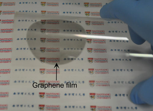 |
| A wafer-sized few-layer graphene film transferred to PET substrate. (Image: Dr. Xiaodong Chen, Nanyang Technological University) |
| "It has been previously demonstrated that iron metal powder can reduce GO into CCG with a substantial removal of oxygen functionalities," Chen explains to Nanowerk. "Therefore, if the metal powder is replaced with the metal foil, large-area CCG films could be fabricated, wherein the metal acts as the reducing agent to convert GO sheets in contact with the metal to CCG sheets as well as the substrate to deposit the film at ambient conditions. Our hypothesis is that the unsteady microenvironment – e.g. hydrophilicity and zeta potential – that is formed around the metal surface triggers the inter-linking of the CCG sheets into a continuous film. |
| Chen points out that the metal substrate plays an important role in determining the growth of graphene films: "CCG films with well-packed layers can readily be grow on nickel, cobalt, iron, and zinc coil, but not on other substrates like lead, tin, platinum, gold, silver, or other nonmetallic substrates," he says. "This is due to the crucial requirement that the substrate metal materials must be active enough to reduce GO." |
| Another important aspect of the new fabrication process is that, by controlling parameters such as time and patterns of metal substrates, CCG films with layer numbers, patterns, doped metal ions, and optical properties can readily be fabricated on demand. |
| The team also demonstrates that the obtained CCG films show high conductivity, mechanical stability, and tunable optical transmittance, showcasing potential application in optoelectronics. |
| Chen is confident that this work will form the precedent for industrial scale production of graphene materials for future applications in electronics and optoelectronics and other functional thin films. He cautions, however, that one challenge to overcome is the tendency of graphene films to ripple – which leads to optical loss and the decrease of transparency, limiting the electronic mobility, and decreasing the chemical stability of the films. Researchers therefore need to find a way to fabricate large-area smooth graphene films under ambient conditions. |
 By
Michael
Berger
– Michael is author of four books by the Royal Society of Chemistry:
Nano-Society: Pushing the Boundaries of Technology (2009),
Nanotechnology: The Future is Tiny (2016),
Nanoengineering: The Skills and Tools Making Technology Invisible (2019), and
Waste not! How Nanotechnologies Can Increase Efficiencies Throughout Society (2025)
Copyright ©
Nanowerk LLC
By
Michael
Berger
– Michael is author of four books by the Royal Society of Chemistry:
Nano-Society: Pushing the Boundaries of Technology (2009),
Nanotechnology: The Future is Tiny (2016),
Nanoengineering: The Skills and Tools Making Technology Invisible (2019), and
Waste not! How Nanotechnologies Can Increase Efficiencies Throughout Society (2025)
Copyright ©
Nanowerk LLC
|

Become a Spotlight guest author! Join our large and growing group of guest contributors. Have you just published a scientific paper or have other exciting developments to share with the nanotechnology community? Here is how to publish on nanowerk.com. |
