| Posted: May 08, 2013 |
Nanoelectronic modeling for noninvasive spatial metrology |
| (Nanowerk Spotlight) State-of-the-art silicon processors, like the Intel Core i5 and i7 found in the latest laptops and tablets, are based on Intel's Ivy Bridge 22 nm technology. In these processors, the smallest structure that the lithography process can provide is around 22 nm. This is less than 100 silicon atoms wide. Or in layman's terms: More than 6 million 22 nm transistors could fit in the period at the end of this sentence. |
| For a transistor to work properly, it must contain impurity atoms – called dopants – replacing the silicon atoms at certain places in the device. Given that modern transistor are approaching the atomic scale, the exact location of a single dopant atom becomes critical in determining the device functionality. |
| In a different context, single dopant atoms in semiconductors have now proved to be an excellent platform to encode quantum information. Therefore, the exact location of single dopant atoms is also crucial to future quantum computers based on silicon. |
| There are a number of techniques to estimate dopants in semiconductors, which be broadly classified as pre-fabrication (estimated prior to manufacturing with software) and post-fabrication (estimated after manufacturing). Prefabrication techniques, although non-invasive, are statistical, which means that there is quite a large uncertainty associated with the resultant dopant positions. Post-fabrication techniques are more accurate, but are generally invasive and destroy a fully functional device in the process. |
| A research team, led by Andrea Morello, an Associate Professor in Quantum Nanosystems at the University of New South Wales in Australia, has now demonstrated a post-fabrication method that has the combined advantage of being non-invasive and precise. This allows the accurate location of a single dopant atom in a nanoscale device, after the device has been fabricated, and without damaging or altering any of its functionalities. |
| The researchers reported their findings in a recent issue of Nano Letters ("Noninvasive Spatial Metrology of Single-Atom Devices"). |
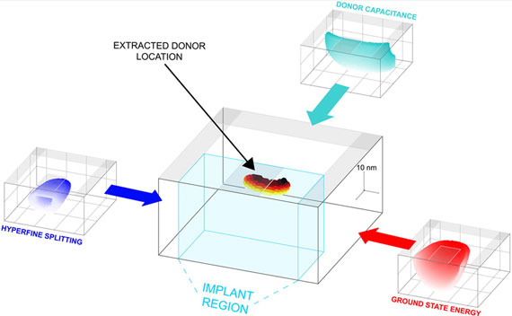 |
| Dopant locations extracted by the metrology technique based on the microscopic modeling of three electrical measurements on a single-atom (phosphorus in silicon) spin qubit device: hyperfine coupling, ground state energy, and capacitive coupling to nearby gates. (Reprinted with permission from American Chemical Society) |
| "We employ a combination of simulation techniques to model three different physical properties of the dopant atom, accessible in an experiment," Fahd Mohiyaddin, the paper's first author, tells Nanowerk. "We then use this information to triangulate the dopant position to ±2.5 nm in two directions and ±15 nm in the third direction." |
| With this technique, the team managed to locate the dopant's possible location to a volume 1500 times smaller than what could have been predicted by prefabrication statistical methods. |
| We obtain the triangulation by combining three different techniques, each one predicting a locus of donor locations compatible with a measurable physical property of the system," explains Mohiyaddin: "First, a classical, finite-elements electrostatic simulation to match the ground state energy of the donor-bound electron; second, a quantum-mechanical tight-binding model for the wave function of the donor-bound electron to match the Stark-shift of the hyperfine coupling; and third, a geometric capacitance extraction method to match the measured capacitive coupling between the donor and the surrounding electrodes." |
| The proposed method is useful for experiments where knowledge of the location/environment of a single dopant atom in a nanostructure is required – provided the electrical characteristics of the dopant can be extracted experimentally. Such scenarios are common in the field of dopant-based quantum computing or for further miniaturizing commercially manufactured transistors. |
| "Very recently, we had the first ever experimental demonstration of a single quantum bit in silicon, encoded in the spin of a dopant atom in silicon," says Mohiyaddin. "The quantum bit was measurable and controllable, thanks to its specific location, but the exact dopant location – to within approximately 3 nm – in the device was not known. The method we have developed has allowed us to determine with high accuracy the location of a 'successful' single dopant, so we can use this information to deterministically place the dopants in the most favorable position in the future." |
| The researchers point out that, both in classical and quantum computing, the exact position of individual atoms will certainly become increasingly important. Experimental methods needed to achieve precise single-dopant placement are being developed both in industry and in basic research. This novel method will help guiding and benchmarking the effort to move classical and quantum electronics closer to the atomic scale. |
 By
Michael
Berger
– Michael is author of four books by the Royal Society of Chemistry:
Nano-Society: Pushing the Boundaries of Technology (2009),
Nanotechnology: The Future is Tiny (2016),
Nanoengineering: The Skills and Tools Making Technology Invisible (2019), and
Waste not! How Nanotechnologies Can Increase Efficiencies Throughout Society (2025)
Copyright ©
Nanowerk LLC
By
Michael
Berger
– Michael is author of four books by the Royal Society of Chemistry:
Nano-Society: Pushing the Boundaries of Technology (2009),
Nanotechnology: The Future is Tiny (2016),
Nanoengineering: The Skills and Tools Making Technology Invisible (2019), and
Waste not! How Nanotechnologies Can Increase Efficiencies Throughout Society (2025)
Copyright ©
Nanowerk LLC
|

Become a Spotlight guest author! Join our large and growing group of guest contributors. Have you just published a scientific paper or have other exciting developments to share with the nanotechnology community? Here is how to publish on nanowerk.com. |
