| Posted: Mar 02, 2006 |
Making Nanotube TVs happen |
| (Nanowerk News) Researchers have turned to carbon nanotubes to create a new class of large area, high resolution, low cost flat panel displays. Some believe field emission display (FED) technology, utilizing carbon nanotubes (CNT) as electron emitter, will be the biggest threat to LCD's dominance in the panel display arena and that FED is the technology of choice for ultra-high definition, wide-screen televisions. |
| FEDs, in a sense, are a hybrid of CRT televisions and LCD televisions. They capitalise on the well-established cathode-anode-phosphor technology built into full-sized CRTs using this in combination with the dot matrix cellular construction of LCDs. The electron emitters, arranged in a grid, are individually controlled by "cold" cathodes (unlike in normal CRTs, field emission does not rely on heating the cathode to boil off electrons) to generate colored light. |
| Field emission display technology makes possible the thin panel of today's liquid crystal displays (LCD), offers a wider field-of-view, provides the high image quality of today's cathode ray tube (CRT) displays, and requires less power than today's CRT displays. |
| Researchers in Taiwan report significant progress in developing a very low-cost fabrication method for the deposition of CNT film for FED applications. Their findings were reported in a paper titled "Fabrication of carbon nanotube field emission cathodes in patterns by a laser transfer method" in the Feb. 7, 2006 online edition of the journal Nanotechnology. |
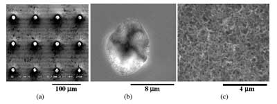 |
| The SEM images showing the patterned carbon nanotube spots. (a) Partial image from a 27 × 27 dot array deposited on an indium-tin-oxide glass substrate. (b) An enlarged image of a particular spot showing that the feature size is about 10 µm. (c) The corresponding enlarged surface image of (b). (Source: National Chung Cheng University; reprinted with permission from IoP Publishing) |
| Jeng-Rong Ho, Professor in the Department of Mechanical Engineering at National Chung Cheng University in Taiwan, explained to Nanowerk that their study proposes a simple and inherently very low cost fabrication method, based on the laser induced forward transfer (LIFT) technique, for the deposition of CNT film for FED applications. The LIFT technique employs laser irradiation to transfer a film initially precoated on an optically transparent support onto a substrate with single laser pulses. |
| "Here, for the first time" says Ho, "employing this technique for FED applications, precision pattern deposition of CNT on a variety of substrates at room temperature and in an ambient environment and also with the feature size down to 10 µm has been achieved." He adds "The lighting test shows that the patterned CNT film exhibits excellent field emission characteristics." |
| FED manufacturing requires CNT to be grown in precise sizes and densities. Height, diameter and tip sharpness affect voltage, while density affects current. But early techniques were rife with technical problems. |
| Researchers incorporated nanotubes into a paste that was placed on a substrate. The haphazard placement of the tubes and their tendency to clump together created spotty illumination. This problem was overcome by growing carbon nanotubes in a specific and orderly manner on substrates using a low-temperature chemical vapor deposition (CVD) process. Low melting temperature, however, excludes the use of the chemical vapour deposition method for growing the large area CNT film directly on substrates. |
| Several alternative approaches have been proposed. The printing based methods and the electrophoretic deposition related methods are two sets of alternatives that attract much industrial attention due to their full scalability and mass production potential. The printing based methods usually use binders or pastes mixing with the CNT that sometimes have problems of tube alignment, uniformity, insufficient outcrop tube density on the surface and possible organic residues. A special surface post-treatment, such as surface rubbing, adhesive taping or laser irradiation, is indispensable. |
| The electrophoretic related methods, although they have shown promise in producing reasonable homogeneity and packing density with controllable film thickness and morphology, require formation from the liquid phase and detailed information on operation has not been reported yet. |
| In their laser-assisted pattern deposition of CNT field emission cathodes on different substrates the Korean researchers achieved favourable emission characteristics, high pattern resolution, with feature size down to 10 µm, high feasibility of using various substrates, good CNT adhesion and fast deposition rate. Furthermore, all steps can be executed in the ambient environment and at low temperature, consequently offering the benefit of potential low cost fabrication of precision pattern deposition. |
|
|
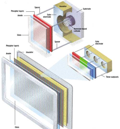 |
| The heart of a FED is an array of CNT-based emitters. A cluster of nanotubes at each emitter act as a cathode to produce electrons via field-emission [top]. Each pixel is composed of three red, green, and blue sub-pixels [right], with their colors combined to create any color. A gate electrode in each sub-pixel creates the electric field for emission. Emitted electrons are swept through a vacuum toward a phosphor by an anode placed between the phosphor and the glass surface of the display [bottom]. Struck by the electrons, the phosphor emits visible light, as in a traditional cathode ray tube, but in a package that’s a fraction the thickness (Source: IEEE Spectrum, September 2003) |
 By
Michael
Berger
– Michael is author of four books by the Royal Society of Chemistry:
Nano-Society: Pushing the Boundaries of Technology (2009),
Nanotechnology: The Future is Tiny (2016),
Nanoengineering: The Skills and Tools Making Technology Invisible (2019), and
Waste not! How Nanotechnologies Can Increase Efficiencies Throughout Society (2025)
Copyright ©
Nanowerk LLC
By
Michael
Berger
– Michael is author of four books by the Royal Society of Chemistry:
Nano-Society: Pushing the Boundaries of Technology (2009),
Nanotechnology: The Future is Tiny (2016),
Nanoengineering: The Skills and Tools Making Technology Invisible (2019), and
Waste not! How Nanotechnologies Can Increase Efficiencies Throughout Society (2025)
Copyright ©
Nanowerk LLC
|

Become a Spotlight guest author! Join our large and growing group of guest contributors. Have you just published a scientific paper or have other exciting developments to share with the nanotechnology community? Here is how to publish on nanowerk.com.
