| Posted: Nov 13, 2007 |
Industrial scale nanotechnology fabrication techniques take shape |
| (Nanowerk Spotlight) Fundamental nanotechnology research in laboratories advances rapidly, as witnessed by the hundreds of new research papers that get published every month. The big bottleneck in getting these new technologies from the lab translated into commercial products is the lack of suitable large-scale fabrication techniques. |
| Almost all laboratory experiments involve elaborate set-ups and are quite tricky processes that require a lot of skill and expertise on part of the researchers. To a large degree, nanotechnology today is more an art than a basis for industrial technologies. Think about a 15th century monk spending 10 years painstakingly writing and painting a single bible - that's where nanotechnology is today; but where we need to get to is something that resembles modern high speed printing machines where you print thousands of books an hour. Take for instance nanowires. |
| Researchers have used nanowires to create transistors like those used in memory devices and prototype sensors for gases or biomolecules. A common approach in the lab is to grow nanowires like blades of grass on a suitable substrate, mow them off and mix them in a fluid to transfer them to a test surface, using some method to give them a preferred orientation. When the carrier fluid dries, the nanowires are left behind like tumbled jackstraws. Using scanning probe microscopy or similar tools, researchers hunt around for a convenient, isolated nanowire to work on, or place electrical contacts without knowing the exact positions of the nanowires. It’s not a technique suitable for mass production. |
| However, researchers have now developed a technique that allows them to selectively grow nanowires on sapphire wafers in specific positions and orientations accurately enough to attach contacts and layer other circuit elements, all with conventional lithography techniques. This fabrication method requires a minimum number of steps and is compatible with today's microelectronics industry. |
| "One of the promises of nanotechnology is nanodevice fabrication from very small building blocks such as nanocrystals" Dr. Babak Nikoobakht explains to Nanowerk. "If you look at the scientific literature there are many, many nanowire growth methods – but methods that are suitable to make large number of nanodevices are as good as nonexistent. At least you can't find any actual examples of mass production anywhere. My motivation was to fill the current gap and convince people that there are other ways to solve the current issues of nanodevice fabrication." |
| Nikoobakht, a researcher at the National Institute of Standards and Technology's (NIST) Surface and Interafce Research Group, has just published a paper in the October 9, 2007 online edition of Chemical Materials where he describes the ability to electrically address the coordinates of millions of horizontally grown nanowires on a given surface ("Toward Industrial-Scale Fabrication of Nanowire-Based Devices"). |
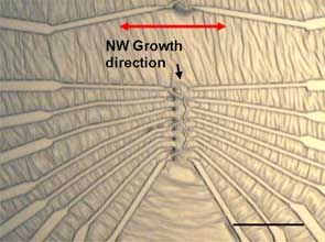 – –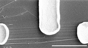 |
| Nanowire electronics: (Left) Optical image shows metal electrodes attached to zinc oxide nanowires using the new technique. Dark spots near the center are the gold pads that start nanowire growth; red arrow shows direction of growth. Scale bar is 50 micrometers long. (Right) Scanning electron microscope image shows electrodes connected to group of nanowires. Scale bar is five micrometers long. (Images: Dr. Nikoobakht, NIST) |
| "Our method allows us to control the nanowire location and its orientation" says Nikoobakht. "Currently, for large scale nanowire device fabrication, it is necessary to grow nanowires in standing positions. These nanowires need to be transferred to a surface and aligned. This requires multistep treatments and brings complexities and inefficiency issues especially when industrial scaling is the goal. Our method has a minimum number of steps. It combines a chemical growth method with well known optical lithography techniques. Nanowires are grown where they need to be." |
| The NIST researchers used conventional semiconductor manufacturing techniques to deposit small amounts of gold in precise locations on a sapphire wafer. In a high-temperature process, the gold deposits bead up into nanodroplets that act as nucleation points for crystals of zinc oxide – a sensor, piezoelectric, UV light emitter, and transparent semiconductor in the visible spectrum – which is a technologically important material. A slight mismatch in the crystal structures of zinc oxide and sapphire induces the semiconductor to grow as a narrow nanowire in one particular direction across the wafer. Because the starting points and the growth direction are both well known, it is relatively straightforward to add electrical contacts and other features with additional lithography steps. |
| This appears to be the first technique that allows nanodevice fabrication on the original position of nanowires and this is done with a combination of a bottom-up chemical approach and conventional optical lithography. It is scalable, i.e., this could be done on 4-6 inch wafers. It is simply because nanowires are horizontal and there is no need to remove, align or treat them. |
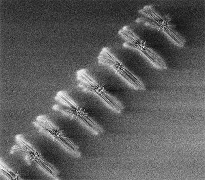 |
| Directed growth of nanowires at predefined locations on a large scale. (Image: Dr. Nikoobakht, NIST). |
| "We have shown that these nanodevices could work as field effect transistors (FET), and that one can make many of them; but at least a year or may be few years is needed to answer all questions about their performance, stability and so on" Nikoobakht explains. "zinc oxide and sapphire are transparent materials in the visible region of the electromagnetic spectrum, people see a strong potential in transparent circuitry and displays for such materials. Sensing is another application, with powerful sensors that are better than the current thin film technology. Light emitters and Flash memory devices would be other applications." |
| Nikoobakht points out that, in order to demonstrate the potentials of this method, the NIST team fabricated nanowire FET devices with one, two, or several nanowires. He also notes that – using this platform – an interesting distinction between electrical properties of individual and ensembles of nanowires was found. |
| Compared to vertical, standing nanowire fabrication techniques, horizontal methods are a fairly new approach and it will take time for other researchers to realize its potential. Nikoobakht is convinced that this method for growing nanocrystals could have quite a significant impact on a wide range of applications such as single photon sources, LEDs, photodetectors, transparent field-effect transistors and displays. |
| "The important part is that nanowires are grown where the devices will be fabricated, and there is no need to transfer nanowires to a different substrate" concludes Nikoobakht. "This approach in its current state seems to be a promising methodology for parallel nanodevice fabrication at technologically relevant scales." |
 By
Michael
Berger
– Michael is author of four books by the Royal Society of Chemistry:
Nano-Society: Pushing the Boundaries of Technology (2009),
Nanotechnology: The Future is Tiny (2016),
Nanoengineering: The Skills and Tools Making Technology Invisible (2019), and
Waste not! How Nanotechnologies Can Increase Efficiencies Throughout Society (2025)
Copyright ©
Nanowerk LLC
By
Michael
Berger
– Michael is author of four books by the Royal Society of Chemistry:
Nano-Society: Pushing the Boundaries of Technology (2009),
Nanotechnology: The Future is Tiny (2016),
Nanoengineering: The Skills and Tools Making Technology Invisible (2019), and
Waste not! How Nanotechnologies Can Increase Efficiencies Throughout Society (2025)
Copyright ©
Nanowerk LLC
|

Become a Spotlight guest author! Join our large and growing group of guest contributors. Have you just published a scientific paper or have other exciting developments to share with the nanotechnology community? Here is how to publish on nanowerk.com. |
